- 您現(xiàn)在的位置:買賣IC網(wǎng) > PDF目錄299403 > LFXP2-40E-6FN484I (LATTICE SEMICONDUCTOR CORP) PDF資料下載
參數(shù)資料
| 型號: | LFXP2-40E-6FN484I |
| 廠商: | LATTICE SEMICONDUCTOR CORP |
| 元件分類: | FPGA |
| 中文描述: | FPGA, 357 MHz, PBGA484 |
| 封裝: | 23 X 23 MM, LEAD FREE, FPBGA-484 |
| 文件頁數(shù): | 77/92頁 |
| 文件大?。?/td> | 1701K |
| 代理商: | LFXP2-40E-6FN484I |
第1頁第2頁第3頁第4頁第5頁第6頁第7頁第8頁第9頁第10頁第11頁第12頁第13頁第14頁第15頁第16頁第17頁第18頁第19頁第20頁第21頁第22頁第23頁第24頁第25頁第26頁第27頁第28頁第29頁第30頁第31頁第32頁第33頁第34頁第35頁第36頁第37頁第38頁第39頁第40頁第41頁第42頁第43頁第44頁第45頁第46頁第47頁第48頁第49頁第50頁第51頁第52頁第53頁第54頁第55頁第56頁第57頁第58頁第59頁第60頁第61頁第62頁第63頁第64頁第65頁第66頁第67頁第68頁第69頁第70頁第71頁第72頁第73頁第74頁第75頁第76頁當前第77頁第78頁第79頁第80頁第81頁第82頁第83頁第84頁第85頁第86頁第87頁第88頁第89頁第90頁第91頁第92頁
4-2
Pinout Information
Lattice Semiconductor
LatticeXP2 Family Data Sheet
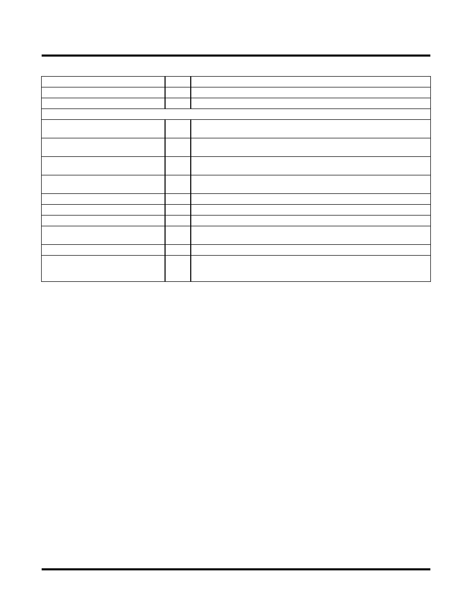
TDO
O
Output pin. Test Data Out pin used to shift data out of a device using 1149.1.
VCCJ
—
Power supply pin for JTAG Test Access Port.
Configuration Pads (Used during sysCONFIG)
CFG[1:0]
I
Mode pins used to specify configuration mode values latched on rising edge
of INITN. During configuration, an internal pull-up is enabled.
INITN
1
I/O
Open Drain pin. Indicates the FPGA is ready to be configured. During config-
uration, a pull-up is enabled.
PROGRAMN
I
Initiates configuration sequence when asserted low. This pin always has an
active pull-up.
DONE
I/O
Open Drain pin. Indicates that the configuration sequence is complete, and
the startup sequence is in progress.
CCLK
I/O
Configuration Clock for configuring an FPGA in sysCONFIG mode.
SISPI
2
I/O
Input data pin in slave SPI mode and Output data pin in Master SPI mode.
SOSPI
2
I/O
Output data pin in slave SPI mode and Input data pin in Master SPI mode.
CSSPIN
2
O
Chip select for external SPI Flash memory in Master SPI mode. This pin has
a weak internal pull-up.
CSSPISN
I
Chip select in Slave SPI mode. This pin has a weak internal pull-up.
TOE
I
Test Output Enable tristates all I/O pins when driven low. This pin has a weak
internal pull-up, but when not used an external pull-up to VCC is recom-
mended.
1. If not actively driven, the internal pull-up may not be sufficient. An external pull-up resistor of 4.7k to 10k
is recommended.
2. When using the device in Master SPI mode, it must be mutually exclusive from JTAG operations (i.e. TCK tied to GND) or the JTAG TCK
must be free-running when used in a system JTAG test environment. If Master SPI mode is used in conjunction with a JTAG download
cable, the device power cycle is required after the cable is unplugged.
Signal Descriptions (Cont.)
Signal Name
I/O
Description
相關(guān)PDF資料 |
PDF描述 |
|---|---|
| LFXP2-17E-7F484C | |
| LFXP20E-3FN484C | |
| LFXP20E-5FN484C | |
| LFXP15C-4FN256C | |
| LFZ3508VXX | GENERAL PURPOSE INDUCTOR |
相關(guān)代理商/技術(shù)參數(shù) |
參數(shù)描述 |
|---|---|
| LFXP2-40E-6FN672C | 功能描述:FPGA - 現(xiàn)場可編程門陣列 40KLUTs 540 I/O Inst -on DSP 1.2V -6 Spd RoHS:否 制造商:Altera Corporation 系列:Cyclone V E 柵極數(shù)量: 邏輯塊數(shù)量:943 內(nèi)嵌式塊RAM - EBR:1956 kbit 輸入/輸出端數(shù)量:128 最大工作頻率:800 MHz 工作電源電壓:1.1 V 最大工作溫度:+ 70 C 安裝風格:SMD/SMT 封裝 / 箱體:FBGA-256 |
| LFXP2-40E-6FN672I | 功能描述:FPGA - 現(xiàn)場可編程門陣列 40K LUTs 540 I/O Ins on DSP 1.2V -6 Spd RoHS:否 制造商:Altera Corporation 系列:Cyclone V E 柵極數(shù)量: 邏輯塊數(shù)量:943 內(nèi)嵌式塊RAM - EBR:1956 kbit 輸入/輸出端數(shù)量:128 最大工作頻率:800 MHz 工作電源電壓:1.1 V 最大工作溫度:+ 70 C 安裝風格:SMD/SMT 封裝 / 箱體:FBGA-256 |
| LFXP240E6IF484C | 制造商:LATTICE 制造商全稱:Lattice Semiconductor 功能描述:LatticeXP2 Family Data Sheet |
| LFXP240E6IF484I | 制造商:LATTICE 制造商全稱:Lattice Semiconductor 功能描述:LatticeXP2 Family Data Sheet |
| LFXP240E6IF672C | 制造商:LATTICE 制造商全稱:Lattice Semiconductor 功能描述:LatticeXP2 Family Data Sheet |
發(fā)布緊急采購,3分鐘左右您將得到回復。