- 您現(xiàn)在的位置:買賣IC網(wǎng) > PDF目錄374284 > K5A3280YBC-T855 (SAMSUNG SEMICONDUCTOR CO. LTD.) MCP MEMORY PDF資料下載
參數(shù)資料
| 型號(hào): | K5A3280YBC-T855 |
| 廠商: | SAMSUNG SEMICONDUCTOR CO. LTD. |
| 英文描述: | MCP MEMORY |
| 中文描述: | MCP的記憶 |
| 文件頁數(shù): | 11/45頁 |
| 文件大?。?/td> | 625K |
| 代理商: | K5A3280YBC-T855 |
第1頁第2頁第3頁第4頁第5頁第6頁第7頁第8頁第9頁第10頁當(dāng)前第11頁第12頁第13頁第14頁第15頁第16頁第17頁第18頁第19頁第20頁第21頁第22頁第23頁第24頁第25頁第26頁第27頁第28頁第29頁第30頁第31頁第32頁第33頁第34頁第35頁第36頁第37頁第38頁第39頁第40頁第41頁第42頁第43頁第44頁第45頁
MCP MEMORY
K5A3x80YT(B)C
Revision 0.0
November 2002
- 11 -
Preliminary
Flash DEVICE OPERATION
Byte/Word Mode
If the BYTE
F
ball is set at logical "1" , the device is in word mode, DQ0-DQ15 are active. Otherwise the BYTE
F
ball is set at logical "0"
, the device is in byte mode, DQ0-DQ7 are active. DQ8-DQ14 are in the High-Z state and DQ15 ball is used as an input for the LSB
(A-1) address ball.
Read Mode
Flash memory is controlled by Chip Enable (CE
F
), Output Enable (OE) and Write Enable (WE). When CE
F
and OE are low and WE
is high, the data stored at the specified address location,will be the output of the device. The outputs are in high impedance state
whenever CE
F
or OE is high.
Standby Mode
Flash memory features Stand-by Mode to reduce power consumption. This mode puts the device on hold when the device is dese-
lected by making CE
F
high (CE
F
= V
IH
). Refer to the DC characteristics for more details on stand-by modes.
Output Disable
The device outputs are disabled when OE is High (OE = V
IH
). The output balls are in high impedance state.
Automatic Sleep Mode
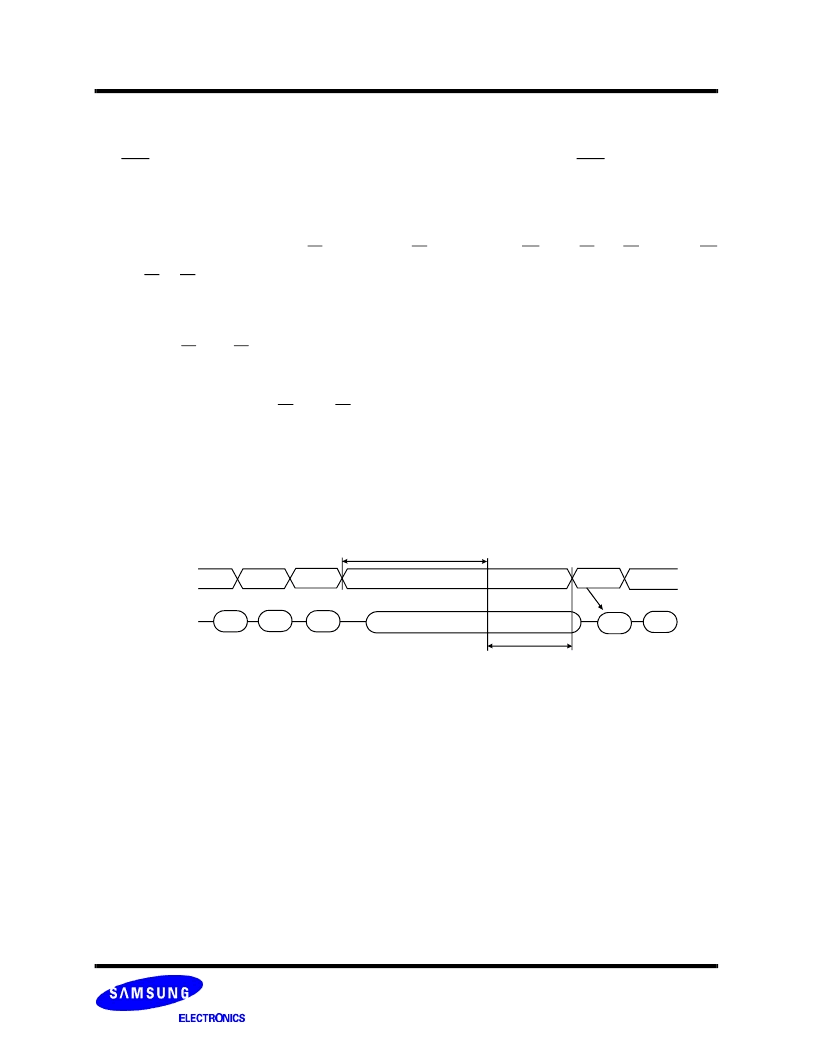
Flash memory features Automatic Sleep Mode to minimize the device power consumption. Since the device typically draws 5
μ
A of
current in Automatic Sleep Mode, this feature plays an extremely important role in battery-powered applications. When addresses
remain steady for t
AA
+50ns, the device automatically activates the Automatic Sleep Mode. In the sleep mode, output data is latched
and always available to the system. When addresses are changed, the device provides new data without wait time.
Data
Outputs
t
AA
+ 50ns
Data
Auto Sleep Mode
Address
Data
Data
Data
Data
Autoselect Mode
Flash memory offers the Autoselect Mode to identify manufacturer and device type by reading a binary code. The Autoselect Mode
allows programming equipment to automatically match the device to be programmed with its corresponding programming algorithm.
In addition, this mode allows the verification of the status of write protected blocks.
The manufacturer and device code can be read
via the command register. The Command Sequence is shown in Table 5 and Figure 3. The autoselect operation of block protect ver-
ification is initiated by first writing two unlock cycle. The third cycle must contain the bank address and autoselect command (90H). If
Block address while (A6, A1, A0) = (0,1,0) is finally asserted on the address ball, it will produce a logical "1" at the device output DQ0
to indicate a write protected block or a logical "0" at the device output DQ0 to indicate a write unprotected block. To terminate the
autoselect operation, write Reset command (F0H) into the command register.
Figure 2. Auto Sleep Mode Operation
相關(guān)PDF資料 |
PDF描述 |
|---|---|
| K5A3280YTC-T755 | MCP MEMORY |
| K5A3280YTC-T855 | MCP MEMORY |
| K5A3380YBC-T755 | MCP MEMORY |
| K5A3380YBC-T855 | MCP MEMORY |
| K5A3380YTC-T755 | MCP MEMORY |
相關(guān)代理商/技術(shù)參數(shù) |
參數(shù)描述 |
|---|---|
| K5A3280YTC-T755 | 制造商:Samsung Electro-Mechanics 功能描述:MCP 32M BIT (4M X 8/2M X 16) DUAL BANK NOR FLASH MEMORY / 8M(1M X 8/512K X 16) FULL CMOS SRAM, PBGA69 |
| K5A3280YTC-T755000 | 制造商:Samsung Electro-Mechanics 功能描述:MCP 32M BIT (4M X 8/2M X 16) DUAL BANK NOR FLASH MEMORY / 8M(1M X 8/512K X 16) FULL CMOS SRAM, PBGA69 |
| K5A3280YTC-T855 | 制造商:SAMSUNG 制造商全稱:Samsung semiconductor 功能描述:MCP MEMORY |
| K5A3340YBC-T755 | 制造商:SAMSUNG 制造商全稱:Samsung semiconductor 功能描述:Multi-Chip Package MEMORY 32M Bit (4Mx8/2Mx16) Dual Bank NOR Flash Memory / 4M(512Kx8/256Kx16) Full CMOS SRAM |
| K5A3340YBC-T855 | 制造商:SAMSUNG 制造商全稱:Samsung semiconductor 功能描述:Multi-Chip Package MEMORY 32M Bit (4Mx8/2Mx16) Dual Bank NOR Flash Memory / 4M(512Kx8/256Kx16) Full CMOS SRAM |
發(fā)布緊急采購,3分鐘左右您將得到回復(fù)。