- 您現(xiàn)在的位置:買賣IC網(wǎng) > PDF目錄385396 > HSP50215 (Intersil Corporation) Digital UpConverter(數(shù)字上變頻器) PDF資料下載
參數(shù)資料
| 型號(hào): | HSP50215 |
| 廠商: | Intersil Corporation |
| 英文描述: | Digital UpConverter(數(shù)字上變頻器) |
| 中文描述: | 數(shù)字上變頻器(數(shù)字上變頻器) |
| 文件頁數(shù): | 11/21頁 |
| 文件大?。?/td> | 162K |
| 代理商: | HSP50215 |

3-11
Cascade Input
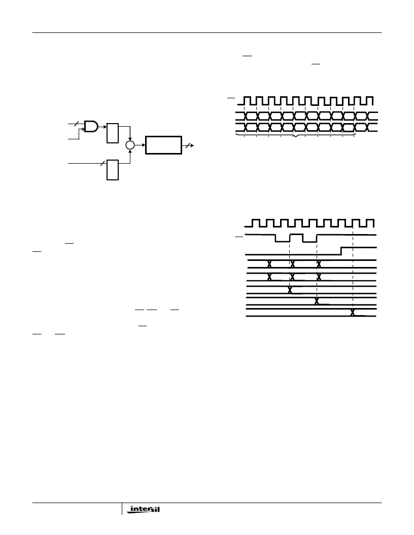
The cascade input allows multiple modulated signals to be
summed together prior to routing to a DAC. Figure 12 is a
block diagram of the cascade circuitry. CAS(15:0) is the
input when cascading with other DUC’s. The CASZ is used
to zero the CAS(15:0) input when it is not used. Both the
CAS(15:0) and the modulator data path are registered, prior
to summation. The output of the summation is saturated to
prevent roll-over.
Output Formatter
The output can be either twos complement or offset binary
format. The OFM signal is used to select the output format.
OFM = 1 is twos complement. OFM = 0 is Offset Binary
format. The OE signal is used to enable the data bus output.
OE = 0 enables the output.
NOTE: The HSP43216 can be used to double the output sample
rate of the DUC, in applications where a higher sample
rate into the DAC is required.
Microprocessor Interface
The microprocessor interface is a memory mapped direct
access interface. The control pins are RD, WR and CE. The
10-bit address bus is A(9:0) [address space is 1024 words]
and the 16-bit data bus is C(15:0). The CE signal gates the
RD and WR. Care must be taken in changing the address
and data lines, as the addresses are updated asynchronous
to REFCLK except in the cases noted in the Microprocessor
Write Section. Most addresses are intended to be
programmed after RESET and before the Start Sequence,
and left alone after that. See the RESET and Start
Sequence sections from more details on initiating operation
of the part.
Reads are asynchronous to clock. The shaping filter
coefficients cannot be read. See the Configuration Control
Register Bit Definitions section for programming details of
the 14 Control Words and the 512 Coefficient Registers.
Microprocessor Write
The Microprocessor Write Interface is used for loading data
into the DUC control registers. Write registers are accessed
via the 10-bit address bus (A9:0) and the 16-bit data bus
(C15:0). The address map for these registers is given in the
Configuration Control Register Bit Definition section.
Configuration data is written into the HSP50215 by setting up
the address (A9:0) and data (C15:0) and generating a rising
edge on WR. A DUC configuration sequence is shown in
Figure 13. Figure 13 assumes that CE is asserted. The filter
coefficients for the shaping filter are loaded in a similar
manner into Control Word addresses 512 - 1023.
The Re-Sampler NCO Center Frequency data is double
buffered and transfers from the Microprocessor Interface
holding registers to the Center Frequency Register on the
assertion of SYNCIN or a Write to Configuration Control
Word 3. The timing waveforms for this process are shown in
Figure 14.
When SYNCIN is sampled “high” by the rising edge of clock,
the contents of the holding registers are transferred to the
Sample Center Frequency Register. Caution should be
taken when using the SYNCIN since the holding register
contents will be transferred to the Sample Center Frequency
Register whenever SYNCIN is asserted (and external sync
is selected via CW22).
Shaping filter I coefficients are loaded from the first coefficient
(C0) in address 0x200h to the last address in 0x2FFh.
Because interpolation by 16 is possible, the coefficient
addresses are structured in blocks of 16, one address for
each phase of the interpolation. With a 256 tap filter using an
interpolation of 16, there are 16 multiplies required to
implement the filter. Tables 4 and 5 detail the coefficient
address allocation, with the Interpolation Phase indicated by
the IP number on the left, and the multiplier number
indicated by the numbers 0 through 15 across the top.
FIGURE 12. CASCADE INPUT BLOCK DIAGRAM
16
16
ALL REGISTERS ARE
CLOCKED AT REFLCK
SATURATE
CIRCUITRY
CAS(15:0)
CASZ
FROM
MODULATOR
16
∑
R
E
G
>
R
E
G
>
FIGURE 13. CONTROL REGISTER LOADING SEQUENCE
WR
2
3
4
5
16
LOAD CONFIGURATION
(10:0)
(15:0)
23
DATA
17
18
19
22
FIGURE 14. RESAMPLER CENTER FREQUENCY CONTROL
REGISTER LOADING SEQUENCE
WR
02
REFCLK
A0-2
C0-7
03
CW02
SYNCIN
MSB
LSB
CW03
SR(29:0)
MSB
LSB
NEW SR
VALUE
HSP50215
相關(guān)PDF資料 |
PDF描述 |
|---|---|
| HSP50216 | Four-Channel Programmable Digital DownConverter(四通道可編程數(shù)字下變頻器) |
| HSP50307 | Burst QPSK Modulator(混合信號(hào)QPSK調(diào)制器) |
| HSP50415VI | CABLE ASSEMBLY; 75 OHM TNC MALE TO 75 OHM TNC MALE; 75 OHM, RG6A/U COAX |
| HSP50415EVAL1 | HSP50415EVAL1 Evaluation Kit |
| HSP9501 | Programmable Data Buffer(可編程數(shù)據(jù)緩沖器) |
相關(guān)代理商/技術(shù)參數(shù) |
參數(shù)描述 |
|---|---|
| HSP50215EVAL | 制造商:INTERSIL 制造商全稱:Intersil Corporation 功能描述:DSP Modulator Evaluation Board |
| HSP50215VC | 制造商:INTERSIL 制造商全稱:Intersil Corporation 功能描述:Digital UpConverter |
| HSP50215VI | 制造商:INTERSIL 制造商全稱:Intersil Corporation 功能描述:Digital UpConverter |
| HSP50216 | 制造商:INTERSIL 制造商全稱:Intersil Corporation 功能描述:Four-Channel Programmable Digital Downconverter |
| HSP50216_06 | 制造商:INTERSIL 制造商全稱:Intersil Corporation 功能描述:Four-Channel Programmable Digital DownConverter |
發(fā)布緊急采購,3分鐘左右您將得到回復(fù)。