- 您現(xiàn)在的位置:買賣IC網(wǎng) > PDF目錄385396 > HSP50307 (Intersil Corporation) Burst QPSK Modulator(混合信號QPSK調(diào)制器) PDF資料下載
參數(shù)資料
| 型號: | HSP50307 |
| 廠商: | Intersil Corporation |
| 英文描述: | Burst QPSK Modulator(混合信號QPSK調(diào)制器) |
| 中文描述: | 突發(fā)QPSK調(diào)制器(混合信號的QPSK調(diào)制器) |
| 文件頁數(shù): | 1/9頁 |
| 文件大小: | 59K |
| 代理商: | HSP50307 |
1
October 2000
HSP50307
Burst QPSK Modulator
Features
256 KBPS Data Rate and 128 KBPS Baud Rate
Burst QPSK Modulation
Programmable Carrier Frequency from 8MHz to
15MHz With a Frequency Step Size of 32kHz
α
= 0.5 Root Raised Cosine (RRC) Filtering For Spec-
trum Shaping
On-Board Synthesizer
Programmable Output Level From 22 to 62dBmV in
1dB Steps
Programmable Charge Pump Current Control
62dBmV Differential Output Driver for 75
Cable
Applications
Burst QPSK Modulator
HSP50307EVAL1 Evaluation Board Is Available
Description
The HSP50307 is a mixed signal burst QPSK Modulator for
upstream CATV Applications. The HSP50307 demultiplexes
and modulates a serial data stream onto an RF Carrier cen-
tered between 8 and 15MHz. The signal spectrum is shaped
with
α
= 0.5 root raised cosine (RRC) digital filters. On-chip fil-
tering limits spurs and harmonics to levels below -35dBc dur-
ing transmissions. The output power level is adjustable over a
40dB range in 1dB steps. The maximum differential output
level is +62dBmV into 75
. A transmitter inhibit function dis-
ables the RF output outside the burst interval. The differential
output amplifier int7-erfaces to the cable via a transformer.
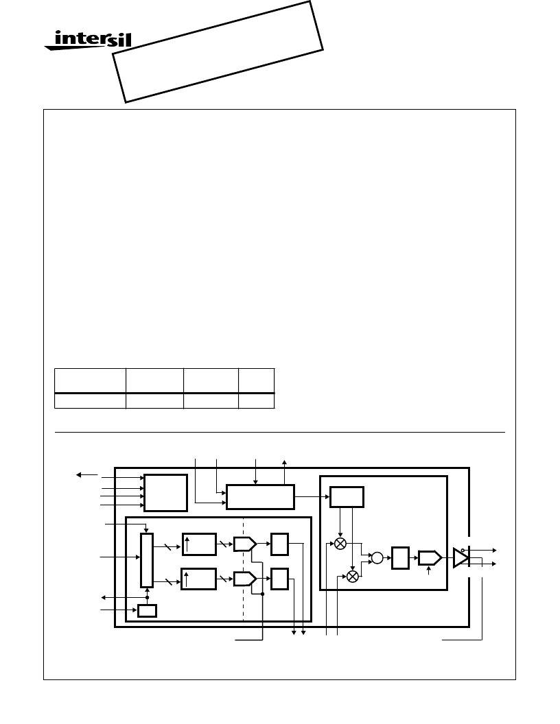
The Block Diagram of the HSP50307 QPSK Modulator is
shown below. The HSP50307 consists of a digital control
interface, an I/Q generator, a synthesizer, and a quadrature
modulator.
The data clock is derived from the master clock. The
HSP50307 demultiplexes the input data bits into in-phase (I)
and quadrature (Q) data streams. The first bit and subsequent
alternating bits of the burst are in-phase data. The two data
streams are filtered, converted from digital to analog, and low
pass filtered to produce the baseband I and Q analog signals.
The baseband signals are up-converted to RF in the Quadra-
ture Modulation Section. The synthesizer provides the local
oscillator (LO) for the quadrature modulator. The frequency is
programmable via the control interface with a resolution of
32kHz. The output of the quadrature modulator is low pass fil-
tered to remove harmonic distortion.
Block Diagram
Ordering Information
PART NUMBER
TEMP.
RANGE (
o
C)
PACKAGE
PKG.
NO.
HSP50307SC
0 to 70
28 Ld SOIC
M28.3
LPF
CONTROL
INTERFACE
RESET
CCLK
MCLK
TXCLK
TX_DATA
TX_EN
C_EN
CDATA
TX_EN
I
Q
8RRC
LPF
8RRC
Q
I
I
Q
9
9
QUAD
GEN
VCO_SET PD_OUT
SYNTHESIZER
/100
D
VCO_IN
RCLK
LPF
PGA
MOD_OUT-
+
DAC_REF
VCM_REF
MCLK MUST ALWAYS BE PRESENT FOR PROPER OPERATION
MOD_OUT+
Indicates analog circuitry.
I/Q GENERATOR
D/A
D/A
QUADRATURE
MODULATOR
File Number
4219.1
CAUTION: These devices are sensitive to electrostatic discharge; follow proper IC Handling Procedures.
1-888-INTERSIL or 321-724-7143
|
Copyright
Intersil Corporation 2000
[ /Title
(HSP5
0307)
/Sub-
ject
(Burst
QPSK
Modu-
lator)
/Autho
r ()
/Key-
words
(Inter-
sil
Corpo-
ration)
/Cre-
ator ()
/DOCI
NFO
pdf-
mark
[
/Page-
Mode
/Use-
Out-
lines
/DOC-
VIEW
pdf-
mark
NO REOBSOLETE PRODUCT
Call or email: centapp@intersil.com
相關(guān)PDF資料 |
PDF描述 |
|---|---|
| HSP50415VI | CABLE ASSEMBLY; 75 OHM TNC MALE TO 75 OHM TNC MALE; 75 OHM, RG6A/U COAX |
| HSP50415EVAL1 | HSP50415EVAL1 Evaluation Kit |
| HSP9501 | Programmable Data Buffer(可編程數(shù)據(jù)緩沖器) |
| HSP9520 | Multilevel Pipeline Registers |
| HSP9520CP | Multilevel Pipeline Registers |
相關(guān)代理商/技術(shù)參數(shù) |
參數(shù)描述 |
|---|---|
| HSP50307_00 | 制造商:INTERSIL 制造商全稱:Intersil Corporation 功能描述:Burst QPSK Modulator |
| HSP50307EVAL1 | 制造商:INTERSIL 制造商全稱:Intersil Corporation 功能描述:2.0GHz to 2.7GHz DownConverter |
| HSP50307SC | 制造商:Rochester Electronics LLC 功能描述:- Bulk |
| HSP5036SC-27 | 制造商:Harris Corporation 功能描述: |
| HSP50415 | 制造商:INTERSIL 制造商全稱:Intersil Corporation 功能描述:Wideband Programmable Modulator (WPM) |
發(fā)布緊急采購,3分鐘左右您將得到回復(fù)。