- 您現(xiàn)在的位置:買賣IC網(wǎng) > PDF目錄375796 > FGH60N6S2 (FAIRCHILD SEMICONDUCTOR CORP) 600V, SMPS II Series N-Channel IGBT PDF資料下載
參數(shù)資料
| 型號: | FGH60N6S2 |
| 廠商: | FAIRCHILD SEMICONDUCTOR CORP |
| 元件分類: | IGBT 晶體管 |
| 英文描述: | 600V, SMPS II Series N-Channel IGBT |
| 中文描述: | 75 A, 600 V, N-CHANNEL IGBT, TO-247 |
| 封裝: | TO-247, 3 PIN |
| 文件頁數(shù): | 2/8頁 |
| 文件大小: | 175K |
| 代理商: | FGH60N6S2 |
2003 Fairchild Semiconductor Corporation
FGH60N6S2 Rev. A2
F
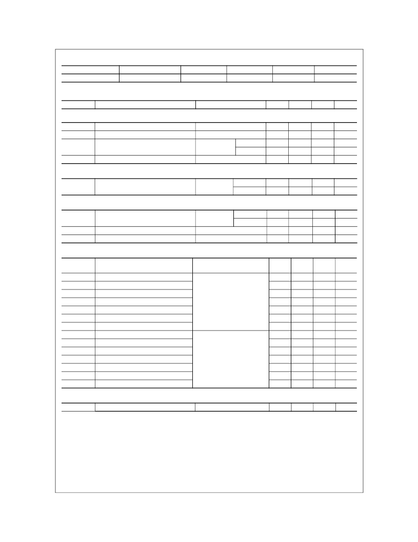
Package Marking and Ordering Information
Electrical Characteristics
T
J
= 25
°
C unless otherwise noted
Off State Characteristics
BV
CES
Collector to Emitter Breakdown Voltage
BV
ECS
Emitter to Collector Breakdown Voltage
I
CES
Collector to Emitter Leakage Current
On State Characteristics
V
CE(SAT)
Collector to Emitter Saturation Voltage
Dynamic Characteristics
Q
G(ON)
Gate Charge
Switching Characteristics
SSOA
Switching SOA
Thermal Characteristics
R
θ
JC
Thermal Resistance Junction-Case
Device Marking
60N6S2
Device
FGH60N6S2
Package
TO-247
Reel Size
Tube
Tape Width
N/A
Quantity
30
Symbol
Parameter
Test Conditions
Min
Typ
Max
Units
I
C
= 250
μ
A, V
GE
= 0
I
C
= -10mA, V
GE
= 0
V
CE
= 600V
600
20
-
-
-
-
-
-
-
-
-
-
V
V
μ
A
mA
nA
T
J
= 25
°
C
T
J
= 125
°
C
250
3
±250
I
GES
Gate to Emitter Leakage Current
V
GE
= ± 20V
I
C
= 40A,
V
GE
= 15V
T
J
= 25
°
C
T
J
= 125
°
C
-
-
1.9
1.65
2.5
2.2
V
V
I
C
= 40A,
V
CE
= 300V
I
C
= 250
μ
A, V
CE
= V
GE
I
C
= 40A, V
CE
= 300V
V
GE
= 15V
V
GE
= 20V
-
-
140
180
4.3
6.5
175
225
5.0
8.0
nC
nC
V
V
V
GE(TH)
V
GEP
Gate to Emitter Threshold Voltage
Gate to Emitter Plateau Voltage
3.5
-
T
J
= 150
°
C, R
G
= 3
,
V
GE
=
15V, L = 100
μ
H, V
CE
= 600V
IGBT and Diode at T
J
= 25
°
C,
I
CE
= 40A,
V
CE
= 390V,
V
GE
= 15V,
R
G
= 3
L = 100
μ
H
Test Circuit - Figure 20
200
-
-
A
t
d(ON)I
t
rI
t
d(OFF)I
t
fI
E
ON1
E
ON2
E
OFF
t
d(ON)I
t
rI
t
d(OFF)I
t
fI
E
ON1
E
ON2
E
OFF
Current Turn-On Delay Time
Current Rise Time
Current Turn-Off Delay Time
Current Fall Time
Turn-On Energy (Note 2)
Turn-On Energy (Note 2)
Turn-Off Energy (Note 3)
Current Turn-On Delay Time
Current Rise Time
Current Turn-Off Delay Time
Current Fall Time
Turn-On Energy (Note 2)
Turn-On Energy (Note 2)
Turn-Off Energy (Note 3)
-
-
-
-
-
-
-
-
-
-
-
-
-
-
18
15
70
50
400
490
310
27
32
110
77
400
750
688
-
-
-
-
-
-
ns
ns
ns
ns
μ
J
μ
J
μ
J
ns
ns
ns
ns
μ
J
μ
J
μ
J
450
-
-
150
90
450
850
950
IGBT and Diode at T
J
= 125
°
C
I
CE
= 40A,
V
CE
= 390V,
V
GE
= 15V,
R
G
= 3
L = 100
μ
H
Test Circuit - Figure 20
TO-247
-
-
0.2
°
C/W
NOTE:
Values for two Turn-On loss conditions are shown for the convenience of the circuit designer. E
is the turn-on loss
of the IGBT only. E
is the turn-on loss when a typical diode is used in the test circuit and the diode is at the same T
J
as the IGBT. The diode type is specified in figure 20.
Turn-Off Energy Loss (E
) is defined as the integral of the instantaneous power loss starting at the trailing edge of
the input pulse and ending at the point where the collector current equals zero (I
= 0A). All devices were tested per
JEDEC Standard No. 24-1 Method for Measurement of Power Device Turn-Off Switching Loss. This test method produc-
es the true total Turn-Off Energy Loss.
相關PDF資料 |
PDF描述 |
|---|---|
| FGK60N6S2D | INDUSTRIAL POWER SUPPLY, 85-265VAC/120-330VDC INPUT, 24V@14A RoHS Compliant: Yes |
| FGL40N120AND | 1200V NPT IGBT |
| FGL40N150 | Electrical Characteristics of the IGBT |
| FGL40N150D | Electrical Characteristics of the IGBT |
| FGL60N100BNTD | NPT-Trench IGBT |
相關代理商/技術參數(shù) |
參數(shù)描述 |
|---|---|
| FGH60N6S2 | 制造商:Fairchild Semiconductor Corporation 功能描述:IGBT N TO-247 |
| FGH75N60SF | 制造商:FAIRCHILD 制造商全稱:Fairchild Semiconductor 功能描述:600V, 75A Field Stop IGBT |
| FGH75N60SFTU | 功能描述:IGBT 晶體管 N-CH/75A 600V FS Planar RoHS:否 制造商:Fairchild Semiconductor 配置: 集電極—發(fā)射極最大電壓 VCEO:650 V 集電極—射極飽和電壓:2.3 V 柵極/發(fā)射極最大電壓:20 V 在25 C的連續(xù)集電極電流:150 A 柵極—射極漏泄電流:400 nA 功率耗散:187 W 最大工作溫度: 封裝 / 箱體:TO-247 封裝:Tube |
| FGH75N60UF | 制造商:FAIRCHILD 制造商全稱:Fairchild Semiconductor 功能描述:600V, 75A Field Stop IGBT |
| FGH75N60UFTU | 功能描述:IGBT 晶體管 N-CH / 600V 75A FS Planar RoHS:否 制造商:Fairchild Semiconductor 配置: 集電極—發(fā)射極最大電壓 VCEO:650 V 集電極—射極飽和電壓:2.3 V 柵極/發(fā)射極最大電壓:20 V 在25 C的連續(xù)集電極電流:150 A 柵極—射極漏泄電流:400 nA 功率耗散:187 W 最大工作溫度: 封裝 / 箱體:TO-247 封裝:Tube |
發(fā)布緊急采購,3分鐘左右您將得到回復。