- 您現(xiàn)在的位置:買賣IC網(wǎng) > PDF目錄375777 > FDMF8705 (FAIRCHILD SEMICONDUCTOR CORP) Driver plus FET Multi-chip Module PDF資料下載
參數(shù)資料
| 型號: | FDMF8705 |
| 廠商: | FAIRCHILD SEMICONDUCTOR CORP |
| 元件分類: | MOSFETs |
| 英文描述: | Driver plus FET Multi-chip Module |
| 中文描述: | HALF BRDG BASED MOSFET DRIVER, QCC56 |
| 封裝: | 8 X 8 MM, ROHS COMPLIANT, MO-220WLLD-5, SMD-56 |
| 文件頁數(shù): | 10/13頁 |
| 文件大小: | 742K |
| 代理商: | FDMF8705 |

10
www.fairchildsemi.com
FDMF8705 Rev. C
F
Typical Application
Application Information
Supply Capacitor Selection
For the supply input (VCIN) of the FDMF8705, a local ceramic
bypass capacitor is recommended to reduce the noise and to
supply the peak current. Use at least a 1μF, X7R or X5R capac-
itor. Keep this capacitor close to the FDMF8705 VCIN and
CGND pins.
Bootstrap Circuit
The bootstrap circuit uses a charge storage capacitor (C
BOOT
)
and the internal diode, as shown in Figure 26. Selection of
these components should be done after the high-side MOSFET
has been chosen. The required capacitance is determined
using the following equation:
where Q
G
is the total gate charge of the high-side MOSFET,
and
V
BOOT
is the voltage droop allowed on the high-side
MOSFET drive. For example, the Q
G
of the internal high-side
MOSFET is about 21nC @ 12V
GS
. For an allowed droop of
~300mV, the required bootstrap capacitance is > 100nF. A good
quality ceramic capacitor must be used.
The average diode forward current, I
F(AVG)
, can be estimated
by:
where f
SW
is the switching frequency of the controller. The peak
surge current rating of the internal diode should be checked
in-circuit, since this is dependent on the equivalent impedance
of the entire bootstrap circuit, including the PCB traces. For
applications requiring higher I
F
, an external diode may be used
in parallel to the internal diode.
Q
G
C
BOOT
>=
(1)
V
BOOT
I
F(AVG)
= Q
G
x f
SW
(2)
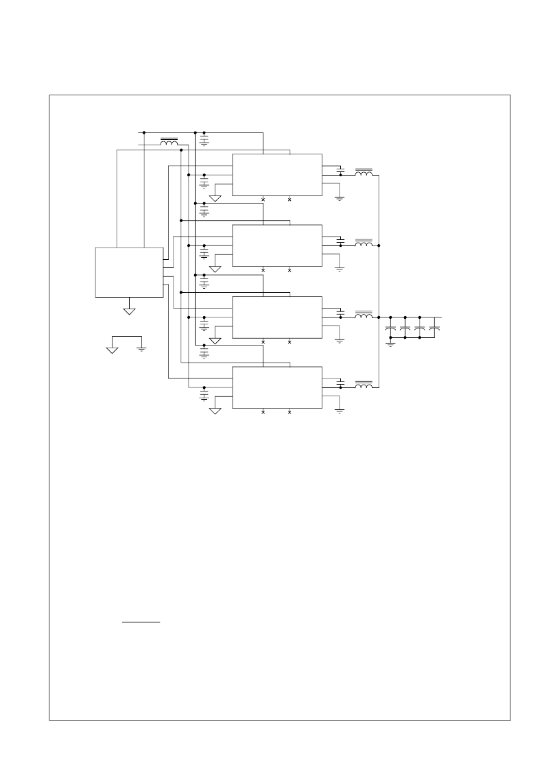
Figure 26. Typical Application
PWM
VIN
CGND
PGND
VCIN
BOOT
VSWH
VCIN 12V
VIN 12V
Signal
GND
LDRV
HDRV
FDMF8705
DISB
PWM
VIN
CGND
PGND
VCIN
BOOT
VSWH
LDRV
HDRV
FDMF8705
DISB
PWM
VIN
CGND
PGND
VCIN
BOOT
VSWH
LDRV
HDRV
FDMF8705
DISB
PWM
VIN
CGND
PGND
VCIN
BOOT
VSWH
LDRV
HDRV
FDMF8705
DISB
PWM3
PWM4
EN
PWM1
PWM2
LDRV
PWM
Controller
VCC
Power
GND
VOUT
相關(guān)PDF資料 |
PDF描述 |
|---|---|
| FDMJ1023PZ | Dual P-Channel PowerTrench㈢ MOSFET |
| FDMS2380 | 740; 38000/740 Series; Microcontroller; Bit Size: 8-bit; ROM: 2K; RAM: 192; ROM Type: QzROM; CPU: 740 core; Minimum Instruction Execution Time (ns): 250 (@8MHz); Operating Frequency / Supply Voltage: 1.8 to 5.5V; Operating Ambient Temperature (°C): -20 to 85; Package Code: PLSP0020JB-A (20P2F-A) |
| FDMS2572_07 | N-Channel UltraFET Trench㈢ MOSFET 150V, 27A, 47mз |
| FDMS2572 | N-Channel UltraFET Trench MOSFET |
| FDMS2672 | N-Channel UltraFET Trench MOSFET 200V, 20A, 77mohm |
相關(guān)代理商/技術(shù)參數(shù) |
參數(shù)描述 |
|---|---|
| FDMH000C11L-YW | 制造商:Thomas & Betts 功能描述:HAZ3FLD,1000W,M.H.,5 TAP BALST |
| FDMHP17C070-YWE | 制造商:Thomas & Betts 功能描述:HZ FDMHP17C070YWE HAZ3,FLD,175W,M.H |
| FDMJ1023PZ | 功能描述:MOSFET -20V Dual P-Channel PowerTrench RoHS:否 制造商:STMicroelectronics 晶體管極性:N-Channel 汲極/源極擊穿電壓:650 V 閘/源擊穿電壓:25 V 漏極連續(xù)電流:130 A 電阻汲極/源極 RDS(導(dǎo)通):0.014 Ohms 配置:Single 最大工作溫度: 安裝風格:Through Hole 封裝 / 箱體:Max247 封裝:Tube |
| FDMJ1027P | 功能描述:MOSFET -20V -2.4A PCH 1.8V SPECIF RoHS:否 制造商:STMicroelectronics 晶體管極性:N-Channel 汲極/源極擊穿電壓:650 V 閘/源擊穿電壓:25 V 漏極連續(xù)電流:130 A 電阻汲極/源極 RDS(導(dǎo)通):0.014 Ohms 配置:Single 最大工作溫度: 安裝風格:Through Hole 封裝 / 箱體:Max247 封裝:Tube |
| FDMJ1028N | 功能描述:MOSFET MLP 20V 3.2A 2.5 VGS NCH S RoHS:否 制造商:STMicroelectronics 晶體管極性:N-Channel 汲極/源極擊穿電壓:650 V 閘/源擊穿電壓:25 V 漏極連續(xù)電流:130 A 電阻汲極/源極 RDS(導(dǎo)通):0.014 Ohms 配置:Single 最大工作溫度: 安裝風格:Through Hole 封裝 / 箱體:Max247 封裝:Tube |
發(fā)布緊急采購,3分鐘左右您將得到回復(fù)。