- 您現(xiàn)在的位置:買賣IC網(wǎng) > PDF目錄375772 > FDD6632 (FAIRCHILD SEMICONDUCTOR CORP) N-Channel Logic Level UltraFET Trench Power MOSFET 30V, 9A, 90mз PDF資料下載
參數(shù)資料
| 型號: | FDD6632 |
| 廠商: | FAIRCHILD SEMICONDUCTOR CORP |
| 元件分類: | JFETs |
| 英文描述: | N-Channel Logic Level UltraFET Trench Power MOSFET 30V, 9A, 90mз |
| 中文描述: | 4 A, 30 V, 0.09 ohm, N-CHANNEL, Si, POWER, MOSFET, TO-252 |
| 封裝: | DPAK-3 |
| 文件頁數(shù): | 7/11頁 |
| 文件大小: | 241K |
| 代理商: | FDD6632 |
2002 Fairchild Semiconductor Corporation
FDD6632
Rev. B
F
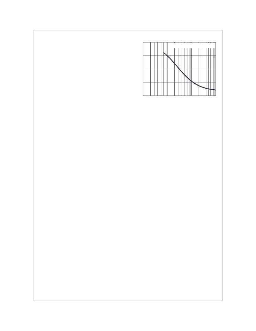
Thermal Resistance vs. Mounting Pad Area
The maximum rated junction temperature, T
JM
, and the
thermal resistance of the heat dissipating path determines
the maximum allowable device power dissipation, P
DM
, in an
application.
Therefore
temperature, T
A
(
o
C), and thermal resistance R
θ
JA
(
o
C/W)
must be reviewed to ensure that T
JM
is never exceeded.
Equation 1 mathematically represents the relationship and
serves as the basis for establishing the rating of the part.
the
application’s
ambient
In using surface mount devices such as the TO-252
package, the environment in which it is applied will have a
significant influence on the part’s current and maximum
power dissipation ratings. Precise determination of P
DM
is
complex and influenced by many factors:
1. Mounting pad area onto which the device is attached and
whether there is copper on one side or both sides of the
board.
2. The number of copper layers and the thickness of the
board.
3. The use of external heat sinks.
4. The use of thermal vias.
5. Air flow and board orientation.
6. For non steady state applications, the pulse width, the
duty cycle and the transient thermal response of the part,
the board and the environment they are in.
Fairchild provides thermal information to assist the
designer’s preliminary application evaluation. Figure 21
defines the R
θ
JA
for the device as a function of the top
copper (component side) area. This is for a horizontally
positioned FR-4 board with 1oz copper after 1000 seconds
of steady state power with no air flow. This graph provides
the necessary information for calculation of the steady state
junction
temperature
or
applications can be evaluated using the Fairchild device
Spice thermal model or manually utilizing the normalized
maximum transient thermal impedance curve.
power
dissipation.
Pulse
Thermal resistances corresponding to other copper areas
can be obtained from Figure 21 or by calculation using
Equation 2. The area, in square inches is the top copper
area including the gate and source pads.
(EQ. 1)
PDM
θ
JA
–
(
-----------------------------
)
=
(EQ. 2)
R
θ
JA
33.32
+
0.268
Area
(
)
-----------23.84
+
=
25
50
75
100
125
0.01
0.1
1
10
Figure 21. Thermal Resistance vs Mounting
Pad Area
R
θ
JA
= 33.32 + 23.84/(0.268+Area)
θ
J
(
o
C
AREA, TOP COPPER AREA (in
2
)
相關(guān)PDF資料 |
PDF描述 |
|---|---|
| FDD6635 | 35V N-Channel PowerTrench MOSFET |
| FDD6637_06 | 35V P-Channel PowerTrench MOSFET |
| FDD6637 | 35V P-Channel PowerTrench-R MOSFET |
| FDD6670S | 20 AMP MINIATURE POWER RELAY |
| FDD6670 | N-Channel, Logic Level, PowerTrench MOSFET |
相關(guān)代理商/技術(shù)參數(shù) |
參數(shù)描述 |
|---|---|
| FDD6632_04 | 制造商:FAIRCHILD 制造商全稱:Fairchild Semiconductor 功能描述:N-Channel Logic Level UltraFET㈢ Trench Power MOSFET 30V, 9A, 70mз |
| FDD6635 | 功能描述:MOSFET 35V N-Ch PowerTrench MOSFET RoHS:否 制造商:STMicroelectronics 晶體管極性:N-Channel 汲極/源極擊穿電壓:650 V 閘/源擊穿電壓:25 V 漏極連續(xù)電流:130 A 電阻汲極/源極 RDS(導(dǎo)通):0.014 Ohms 配置:Single 最大工作溫度: 安裝風(fēng)格:Through Hole 封裝 / 箱體:Max247 封裝:Tube |
| FDD6637 | 功能描述:MOSFET 35V PCH PowerTrench MOSFET RoHS:否 制造商:STMicroelectronics 晶體管極性:N-Channel 汲極/源極擊穿電壓:650 V 閘/源擊穿電壓:25 V 漏極連續(xù)電流:130 A 電阻汲極/源極 RDS(導(dǎo)通):0.014 Ohms 配置:Single 最大工作溫度: 安裝風(fēng)格:Through Hole 封裝 / 箱體:Max247 封裝:Tube |
| FDD6637 | 制造商:Fairchild Semiconductor Corporation 功能描述:P-CHANNEL POWERTRENCH MOSFET 制造商:Fairchild Semiconductor Corporation 功能描述:P CHANNEL MOSFET, -35V, 13A, TO-252 |
| FDD6637_06 | 制造商:FAIRCHILD 制造商全稱:Fairchild Semiconductor 功能描述:35V P-Channel PowerTrench MOSFET |
發(fā)布緊急采購,3分鐘左右您將得到回復(fù)。