- 您現(xiàn)在的位置:買賣IC網(wǎng) > PDF目錄384280 > EDE5116AJBG (Elpida Memory, Inc.) 512M bits DDR2 SDRAM PDF資料下載
參數(shù)資料
| 型號(hào): | EDE5116AJBG |
| 廠商: | Elpida Memory, Inc. |
| 英文描述: | 512M bits DDR2 SDRAM |
| 中文描述: | 512M比特DDR2 SDRAM內(nèi)存 |
| 文件頁(yè)數(shù): | 38/77頁(yè) |
| 文件大小: | 589K |
| 代理商: | EDE5116AJBG |
第1頁(yè)第2頁(yè)第3頁(yè)第4頁(yè)第5頁(yè)第6頁(yè)第7頁(yè)第8頁(yè)第9頁(yè)第10頁(yè)第11頁(yè)第12頁(yè)第13頁(yè)第14頁(yè)第15頁(yè)第16頁(yè)第17頁(yè)第18頁(yè)第19頁(yè)第20頁(yè)第21頁(yè)第22頁(yè)第23頁(yè)第24頁(yè)第25頁(yè)第26頁(yè)第27頁(yè)第28頁(yè)第29頁(yè)第30頁(yè)第31頁(yè)第32頁(yè)第33頁(yè)第34頁(yè)第35頁(yè)第36頁(yè)第37頁(yè)當(dāng)前第38頁(yè)第39頁(yè)第40頁(yè)第41頁(yè)第42頁(yè)第43頁(yè)第44頁(yè)第45頁(yè)第46頁(yè)第47頁(yè)第48頁(yè)第49頁(yè)第50頁(yè)第51頁(yè)第52頁(yè)第53頁(yè)第54頁(yè)第55頁(yè)第56頁(yè)第57頁(yè)第58頁(yè)第59頁(yè)第60頁(yè)第61頁(yè)第62頁(yè)第63頁(yè)第64頁(yè)第65頁(yè)第66頁(yè)第67頁(yè)第68頁(yè)第69頁(yè)第70頁(yè)第71頁(yè)第72頁(yè)第73頁(yè)第74頁(yè)第75頁(yè)第76頁(yè)第77頁(yè)
EDE5108AJBG, EDE5116AJBG
Preliminary Data Sheet E1044E20 (Ver. 2.0)
38
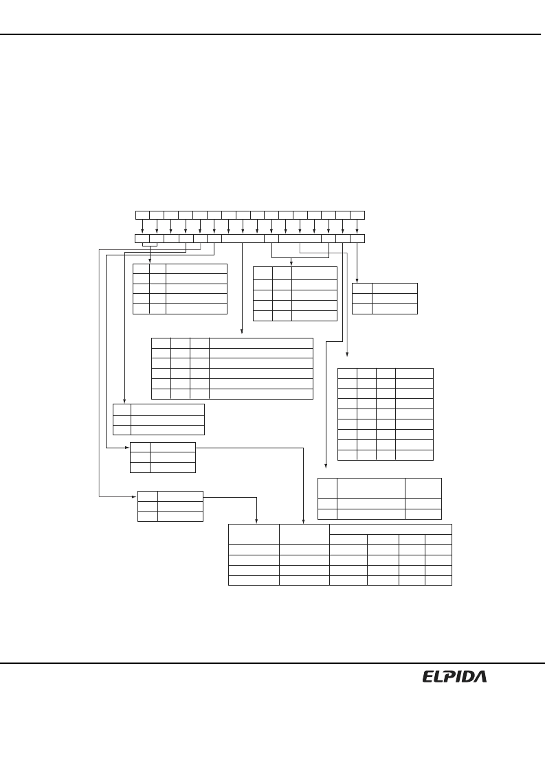
DDR2 SDRAM Extended Mode Registers Set [EMRS]
EMRS (1) Programming
The extended mode register (1) stores the data for enabling or disabling the DLL, output driver strength, additive
latency, ODT, /DQS disable, OCD program, RDQS enable. The default value of the extended mode register (1) is
not defined, therefore the extended mode register (1) must be written after power-up for proper operation. The
extended mode register (1) is written by asserting low on /CS, /RAS, /CAS, /WE, high on BA0 and low on BA1, while
controlling the states of address pins A0 to A13. The DDR2 SDRAM should be in all banks precharge with CKE
already high prior to writing into the extended mode register (1). The mode register set command cycle time (tMRD)
must be satisfied to complete the write operation to the extended mode register (1). Mode register contents can be
changed using the same command and clock cycle requirements during normal operation as long as all banks are in
the precharge state. A0 is used for DLL enable or disable. A1 is used for enabling a half strength output driver. A3
to A5 determines the additive latency, A7 to A9 are used for OCD control, A10 is used for /DQS disable and A11 is
used for RDQS enable. A2 and A6 are used for ODT setting.
Notes: 1. A13 is reserved for future use, and must be programmed to 0 when setting the extended mode register.
2 When adjust mode is issued, AL from previously set value must be applied.
3. After setting to default, OCD mode needs to be exited by setting A9 to A7 to 000.
Refer to the chapter Off-Chip Driver (OCD)Impedance Adjustment for detailed information.
4. Output disabled - DQ, DQS, /DQS, RDQS, /RDQS. This feature is used in conjunction with DIMM
IDD measurements when IDDQ is not desired to be included.
EMRS (1)
A13
BA0
BA1
A12 A11 A10
A9
A8
A7
A6
A5
A4
A3
A2
A1
A0
Address field
A11
0
1
RDQS enable
Disable
Enable
1
0
0
*
/DQS
OCD program
Rtt Additive latency Rtt D.I.C DLL
Extended mode register
A10
0
1
/DQS enable
Enable
Disable
A5
0
0
0
0
1
1
1
1
Additive latency
A4
0
0
1
1
0
0
1
1
A3
0
1
0
1
0
1
0
1
Latency
0
1
2
3
4
5
Reserved
Reserved
A0
0
1
DLL enable
Enable
Disable
BA1
0
0
1
1
MRS mode
MRS
EMRS(1)
EMRS(2)
EMRS(3): Reserved
A6
0
0
1
1
A2
0
1
0
1
Rtt (nominal )
ODT Disabled
75
Ω
150
Ω
50
Ω
A9
0
0
0
1
1
Driver impedance adjustment
A8
0
0
1
0
1
A7
0
1
0
0
1
OCD calibration mode exit
Drive(1)
Drive(0)
Adjust mode*
OCD Calibration default*
A1
0
1
Driver strength control
Output driver
impedance control
Normal
Weak
Driver
size
100%
60%
A11
(RDQS enable)
0 (Disable)
0 (Disable)
1 (Enable)
1 (Enable)
A10
(/DQS enable)
0 (Enable)
1 (Disable)
0 (Enable)
1 (Disable)
RDQS/DM
DM
DM
RDQS
RDQS
/RDQS
High-Z
High-Z
/RDQS
High-Z
DQS
DQS
DQS
DQS
DQS
/DQS
/DQS
High-Z
/DQS
High-Z
Operation
1
2
3
RDQS
Qoff
BA0
0
1
0
1
A12
0
1
Qoff*
Output buffers enabled
Output buffers disabled
Strobe function matrix
4
相關(guān)PDF資料 |
PDF描述 |
|---|---|
| EDE5116AJBG-6E-E | 512M bits DDR2 SDRAM |
| EDE5116AJBG-8E-E | 512M bits DDR2 SDRAM |
| EDE702 | Serial LCD Interface IC |
| EDI8808CB | HIGH SPEED, LOW POWER 64K MONOLITHIC SRAM |
| EDI8F32256C | HIGH SPEED EIGHT MEGABIT SRAM MODULE |
相關(guān)代理商/技術(shù)參數(shù) |
參數(shù)描述 |
|---|---|
| EDE5116AJBG-1J | 制造商:ELPIDA 制造商全稱:Elpida Memory 功能描述:512M bits DDR2 SDRAM |
| EDE5116AJBG-1J-E | 制造商:ELPIDA 制造商全稱:Elpida Memory 功能描述:512M bits DDR2 SDRAM |
| EDE5116AJBG-6E-E | 制造商:ELPIDA 制造商全稱:Elpida Memory 功能描述:512M bits DDR2 SDRAM |
| EDE5116AJBG-6ELI-E | 制造商:ELPIDA 制造商全稱:Elpida Memory 功能描述:512M bits DDR2 SDRAM WTR (Wide Temperature Range) |
| EDE5116AJBG-8E-E | 制造商:ELPIDA 制造商全稱:Elpida Memory 功能描述:512M bits DDR2 SDRAM |
發(fā)布緊急采購(gòu),3分鐘左右您將得到回復(fù)。