- 您現(xiàn)在的位置:買賣IC網(wǎng) > PDF目錄4573 > DS1865T+T&R (Maxim Integrated Products)IC PON CONTROL TRI 28-TQFN PDF資料下載
參數(shù)資料
| 型號: | DS1865T+T&R |
| 廠商: | Maxim Integrated Products |
| 文件頁數(shù): | 44/67頁 |
| 文件大小: | 0K |
| 描述: | IC PON CONTROL TRI 28-TQFN |
| 產(chǎn)品培訓(xùn)模塊: | Lead (SnPb) Finish for COTS Obsolescence Mitigation Program |
| 標(biāo)準(zhǔn)包裝: | 2,500 |
| 系列: | * |
| 類型: | * |
| 應(yīng)用: | * |
| 安裝類型: | 表面貼裝 |
| 封裝/外殼: | 28-WFQFN 裸露焊盤 |
| 供應(yīng)商設(shè)備封裝: | 28-TQFN-EP(5x5) |
| 包裝: | 帶卷 (TR) |
第1頁第2頁第3頁第4頁第5頁第6頁第7頁第8頁第9頁第10頁第11頁第12頁第13頁第14頁第15頁第16頁第17頁第18頁第19頁第20頁第21頁第22頁第23頁第24頁第25頁第26頁第27頁第28頁第29頁第30頁第31頁第32頁第33頁第34頁第35頁第36頁第37頁第38頁第39頁第40頁第41頁第42頁第43頁當(dāng)前第44頁第45頁第46頁第47頁第48頁第49頁第50頁第51頁第52頁第53頁第54頁第55頁第56頁第57頁第58頁第59頁第60頁第61頁第62頁第63頁第64頁第65頁第66頁第67頁
DS1865
PON Triplexer Control and
Monitoring Circuit
____________________________________________________________________
49
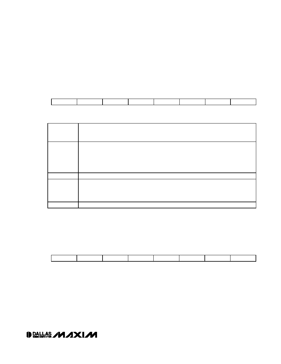
Table 02h, Register 89h: Config
FACTORY DEFAULT
00h
READ ACCESS
PW2
WRITE ACCESS
PW2
MEMORY TYPE:
Nonvolatile (SEE)
89h
FETG DIR
TX-F EN
RESERVED
ASEL
RESERVED
bit7
bit0
Configure the memory location and the polarity of the digital outputs.
bit7
FETG DIR: Chooses the direction or polarity of the FETG output for normal operation.
0 = (Default) Under normal operation, FETG is pulled low. Intended for use with nMOS.
1 = Under normal operation, FETG is pulled high. Intended for use with pMOS.
bit6
TX-F EN: The TX-F output pin always reflects the wired-OR of all TXF enabled alarm states. This bit
will enable the latching of the alarm state for the TXF output pin.
0 = (Default) Not latched.
1 = The alarm bits are latched until cleared by a TX-D transition or power-down. If VCC_Lo_Alarm is
enabled for either FETG or TX-F then latching is disabled until the after the first VCC measurement is
made above the VCC_Lo set point to allow for proper operation during slow power-on cycles.
bit5
RESERVED
bit4
ASEL: Address Select.
0 = (Default) Device Address of A2h.
1 = I2C slave address is determined by the value programmed in the DEVICE ADDRESS byte
(Table 02h, Register 8Ch).
bit3:0
RESERVED
Table 02h, Register 8Ah: Startup Step
FACTORY DEFAULT:
00h
READ ACCESS
PW2
WRITE ACCESS
PW2
MEMORY TYPE:
Nonvolatile (SEE)
8Ah
2
12
2
11
2
10
2
9
2
8
2
7
2
6
2
5
bit7
bit0
This value will define the maximum allowed step for the upper 8 bits of IBIAS output during startup. Programming this value to 00h
cause the device to take single LSB (2
0) steps towards convergence. See the BIAS and MOD Output During Power-Up section for
details.
相關(guān)PDF資料 |
PDF描述 |
|---|---|
| TLE8264E | IC SYSTEM BASIS CHIP DSO-36 |
| MAX4507CWN+T | IC SIGNAL LINE PROTECTOR 18-SOIC |
| TLE8263-2E | IC SYSTEM BASIS CHIP DSO-36 |
| TLE8263E | IC SYSTEM BASIS CHIP DSO-36 |
| TLE8262E | IC SYSTEM BASIS CHIP DSO-36 |
相關(guān)代理商/技術(shù)參數(shù) |
參數(shù)描述 |
|---|---|
| DS1866 | 功能描述:數(shù)字電位計 IC RoHS:否 制造商:Maxim Integrated 電阻:200 Ohms 溫度系數(shù):35 PPM / C 容差:25 % POT 數(shù)量:Dual 每 POT 分接頭:256 弧刷存儲器:Volatile 緩沖刷: 數(shù)字接口:Serial (3-Wire, SPI) 描述/功能:Dual Volatile Low Voltage Linear Taper Digital Potentiometer 工作電源電壓:1.7 V to 5.5 V 電源電流:27 uA 最大工作溫度:+ 125 C 安裝風(fēng)格:SMD/SMT 封裝 / 箱體:TQFN-16 封裝:Reel |
| DS1866+ | 功能描述:數(shù)字電位計 IC Log Trimmer RoHS:否 制造商:Maxim Integrated 電阻:200 Ohms 溫度系數(shù):35 PPM / C 容差:25 % POT 數(shù)量:Dual 每 POT 分接頭:256 弧刷存儲器:Volatile 緩沖刷: 數(shù)字接口:Serial (3-Wire, SPI) 描述/功能:Dual Volatile Low Voltage Linear Taper Digital Potentiometer 工作電源電壓:1.7 V to 5.5 V 電源電流:27 uA 最大工作溫度:+ 125 C 安裝風(fēng)格:SMD/SMT 封裝 / 箱體:TQFN-16 封裝:Reel |
| DS1866N | 制造商:未知廠家 制造商全稱:未知廠家 功能描述:Interface IC |
| DS1866S | 制造商:未知廠家 制造商全稱:未知廠家 功能描述:Interface IC |
| DS1866SN | 制造商:未知廠家 制造商全稱:未知廠家 功能描述:Interface IC |
發(fā)布緊急采購,3分鐘左右您將得到回復(fù)。