- 您現(xiàn)在的位置:買賣IC網(wǎng) > PDF目錄376632 > DEM-VSP2232Y (Texas Instruments, Inc.) CCD SIGNAL PROCESSOR FOR DIGITAL CAMERAS PDF資料下載
參數(shù)資料
| 型號(hào): | DEM-VSP2232Y |
| 廠商: | Texas Instruments, Inc. |
| 英文描述: | CCD SIGNAL PROCESSOR FOR DIGITAL CAMERAS |
| 中文描述: | CCD信號(hào)處理器的數(shù)碼相機(jī) |
| 文件頁(yè)數(shù): | 4/19頁(yè) |
| 文件大小: | 248K |
| 代理商: | DEM-VSP2232Y |
第1頁(yè)第2頁(yè)第3頁(yè)當(dāng)前第4頁(yè)第5頁(yè)第6頁(yè)第7頁(yè)第8頁(yè)第9頁(yè)第10頁(yè)第11頁(yè)第12頁(yè)第13頁(yè)第14頁(yè)第15頁(yè)第16頁(yè)第17頁(yè)第18頁(yè)第19頁(yè)
VSP2232
SLAS320
–
MAY 2001
4
www.ti.com
Terminal Functions (continued)
TERMINAL
TYPE
DESCRIPTION
NAME
SLOAD
VCC
Designators in TYPE column: P
–
power supply and ground, DI
–
digital input, DO
–
digital output, AI
–
aAnalog input, AO
–
analog output
NO.
46
DI
P
Serial data latch signal (triggered at the rising edge)
Analog power supply
18, 24, 27, 33, 34, 40
detailed description
introduction
The VSP2232 is a complete mixed-signal IC that contains all of the key features associated with the processing
of the CCD imager output signal in a video camera, a digital still camera, a security camera, or similar
applications. A simplified block diagram is shown on the front page of this data sheet. The VSP2232 includes
a correlated double sampler (CDS), a programmable gain amplifier (PGA), an analog-to-digital converter
(ADC), an input clamp, an optical black (OB) level clamp loop, a serial interface, a timing control, and a reference
voltage generator. We recommend an off-chip emitter follower buffer between the CCD output and the VSP2232
CCDIN input. The PGA gain control, the clock polarity setting, and the operation mode choosing can be made
through the serial interface. All parameters are reset to the default value when the RESET pin goes to low
asynchronously from the clocks.
correlated double sampler (CDS)
The output signal of a CCD imager is sampled twice during one pixel period, one at the reference interval and
the other at the data interval.
Subtracting these two samples, extracts the video information of the pixel as well as removes any noise that
is common
—
or correlated
—
to both the intervals.
Thus, a CDS is very important to reduce the reset noise and the low frequency noises that are present on the
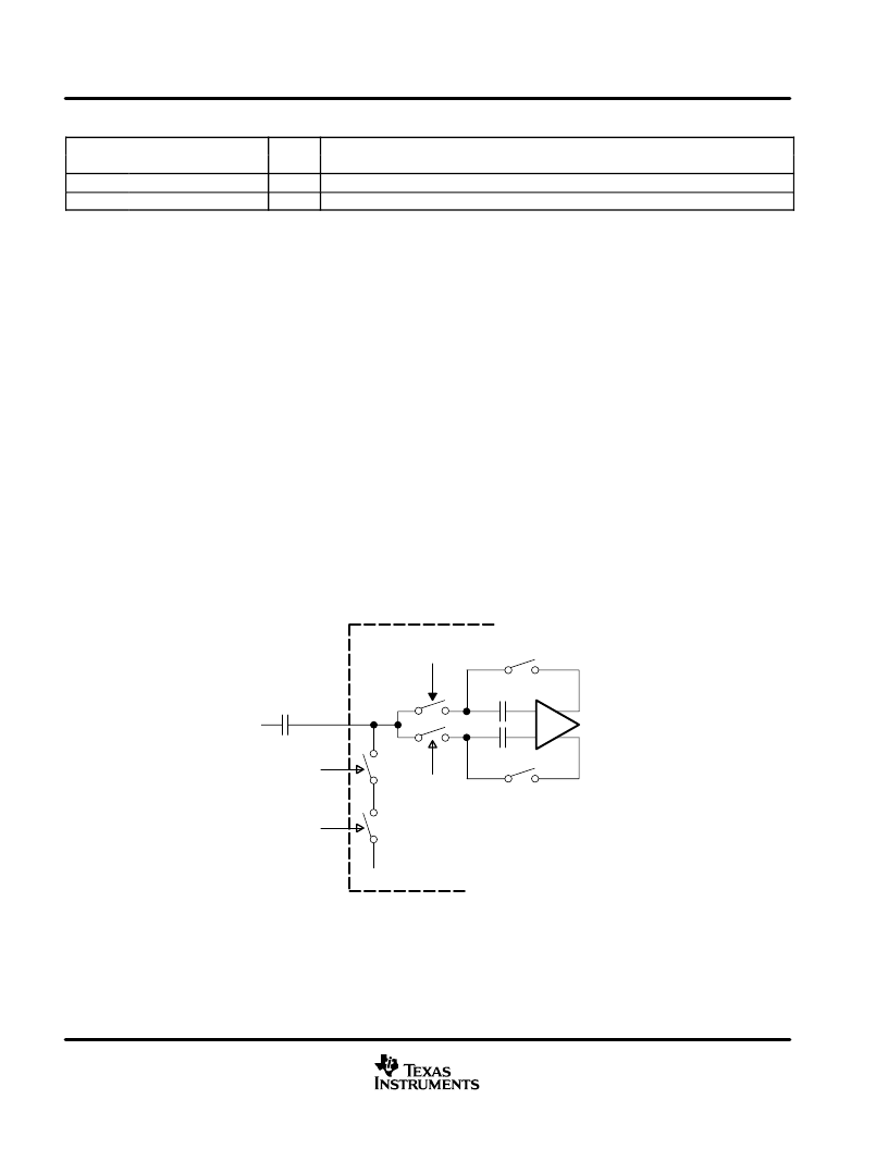
CCD output signal. Figure 1 shows the simplified block diagram of the CDS and input clamp.
_
+
OPA
C(1) = 5 pF
C(2) = 5 pF
SHP
SHD
REFN (1.25 V)
VSP2232
CCDIN
CLPDM
SHP
CIN
CCD
Output
Figure 1. Simplified Block Diagram of CDS and Input Clamp
The CDS is driven through an off-chip coupling capacitor (C
IN
). AC coupling is strongly recommended because
the DC level of the CCD output signal is usually too high (several volts) for the CDS to work properly. A 0.1-
μ
F
capacitor is recommended for C
IN
, however, it depends on the application environment.
相關(guān)PDF資料 |
PDF描述 |
|---|---|
| DEM16101H | LCD MODULE |
| DEM16101SYH | DEM16101SYH |
| DEM16216SYH-LY | DEM16216SYH-LY |
| DEM16216SYH-PY | Display Elektronik GmbH |
| DEM16217SYH | Display Elektronik GmbH |
相關(guān)代理商/技術(shù)參數(shù) |
參數(shù)描述 |
|---|---|
| DEM-VSP2260Y | 制造商:Rochester Electronics LLC 功能描述:- Bulk |
| DEM-VSP2262Y | 制造商:Texas Instruments 功能描述:EVAL BD FOR CCD SGNL PROCESSOR FOR DGTL CAMERAS - Bulk |
| DEM-VSP3100Y | 制造商:Texas Instruments 功能描述:EVALUATION/DEMO BOARD FOR VSP3100Y - Bulk |
| DEMX-5W1P-1AON-K87 | 制造商:ITT Interconnect Solutions 功能描述:DEMX-5W1P-1AON-K87 - Bulk |
| DEMX5W1PK87 | 制造商:ITT 功能描述:DSUB 5W1 M PCR/A G50 T 制造商:ITT Interconnect Solutions 功能描述:DSUB 5W1 M PCR/A G50 T |
發(fā)布緊急采購(gòu),3分鐘左右您將得到回復(fù)。