- 您現(xiàn)在的位置:買賣IC網(wǎng) > PDF目錄375330 > AND8020 (Analog Devices, Inc.) Termination of ECL Logic Devices with EF (Emitter Follower) OUTPUT Structure PDF資料下載
參數(shù)資料
| 型號: | AND8020 |
| 廠商: | Analog Devices, Inc. |
| 英文描述: | Termination of ECL Logic Devices with EF (Emitter Follower) OUTPUT Structure |
| 中文描述: | ECL邏輯器件的終止與英法(發(fā)射極跟隨器)輸出結(jié)構(gòu) |
| 文件頁數(shù): | 7/18頁 |
| 文件大?。?/td> | 168K |
| 代理商: | AND8020 |
AND8020/D
http://onsemi.com
7
Table C. Y Term Table
|V
CC
V
EE
| = 5.0 V
|V
CC
V
EE
| = 3.3 V
|V
CC
V
EE
| = 2.5 V
Z
0
R
t1
R
t2
R
t3
Z
0
R
t1
R
t2
R
t3
Z
0
R
t1
R
t2
R
t3
50
50
50
112
50
50
50
46
50
50
50
21.2
70
70
70
156
70
70
70
64
70
70
70
29.7
75
75
75
166
75
75
75
68
75
75
75
31.8
80
80
80
179
80
80
80
72
80
80
80
33.9
90
90
90
201
90
90
90
82
90
90
90
38.1
100
100
100
223
100
100
100
91
100
100
100
42.4
120
120
120
268
120
120
120
109
120
120
120
50.8
150
150
150
335
150
150
150
136
150
150
150
63.6
V
EE
R
E
R
E
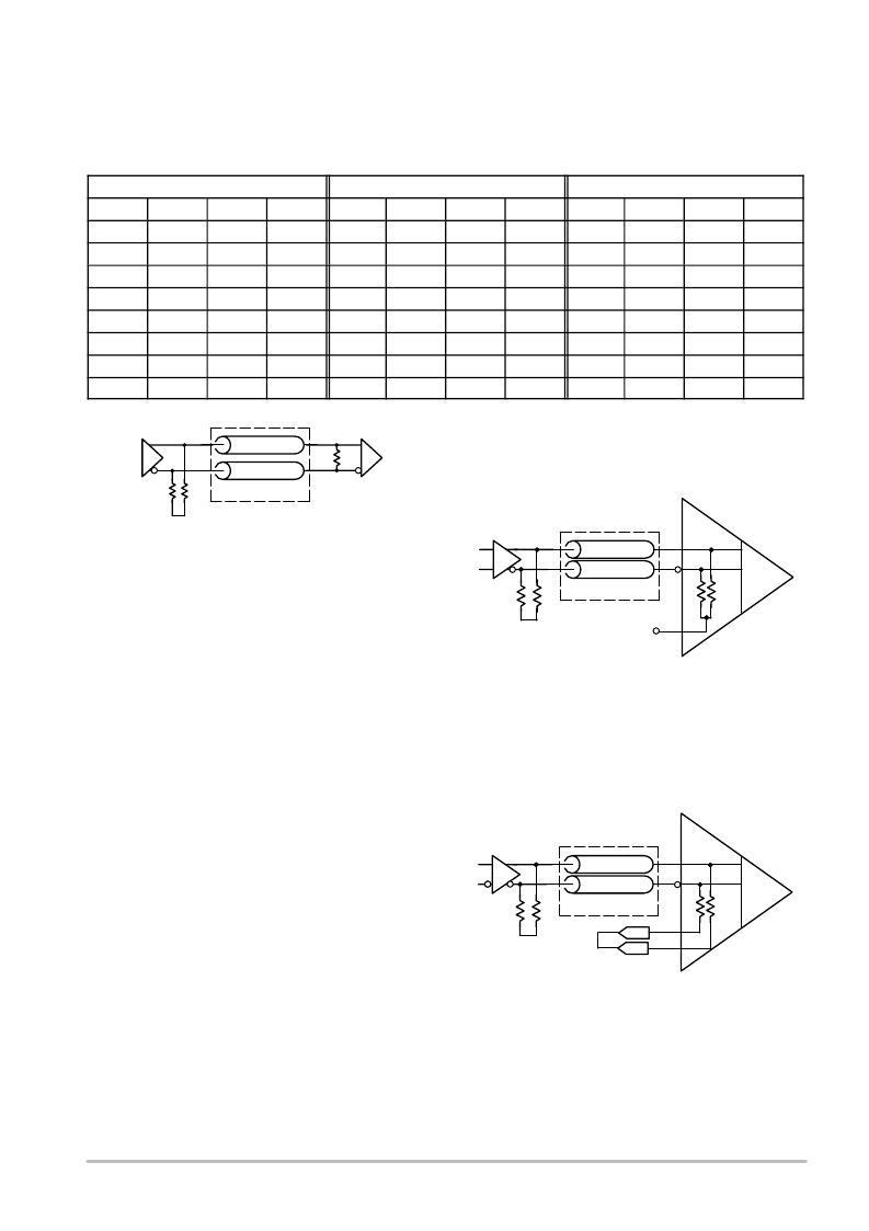
Figure 7. Standard Pair with External Parallel
R
t
(*or twisted pair)
*TLine Z
0
*TLine Z
0
Near DC Current Return Standard Pair
Termination
The standard pair termination scheme uses a pulldown
resistor, R
E
, located at each driver pin to return the output
transistor bias current near the driver, and an impedance
matching parallel resistor, R
T
, located at the receiver input
pins (see Figure 7, standard pair with external parallel, and
Figure 8, standard pair termination with internal
termination, and Figure 9, standard pair termination with
singulated internal termination resistors). The impedance
matching parallel resistor may be internal or external
depending on the receiver device. If internal to the receiver,
the resistor may be singulated or combined (“combo”) for
external pinout.
The diagram of Figure 7 shows a Standard Pair
Termination with an R
E
resistor for DC output current bias
located nearby each driver pin: refer to Table B, for values
of R
E
. The differential transmission line AC impedance
matching resistance, R
t
, is located externally near the
receiver input pins.
As a variation of a Standard Pair Termination, a receiver
may provide the differential transmission line AC
impedance matching resistance, R
t
, internally. This internal
impedance matching termination may be pinned out either
combined into a Combo V
t
pin or each resistor may be
singulated and pinned out, such as V
t1
and V
t2
.
When left open, the Combo Pin still provides a passive
100
termination across the nearby receiver’s differential
signal line pair. This can compliment a pulldown resistor, R
E
,
located on each line of a differential at the driver pins. This is
illustrated in Figure 8.
Figure 8. Standard Pair Termination with
Internal Termination
Open V
t
Pin
R
R
(*or twisted pair)
Driver
Receiver
*TLine Z
0
*TLine Z
0
Internal Termination Combo Pin
V
EE
R
E
R
E
When the Internal Termination resistors are singulated,
the two V
t
pins must be shorted to create the 100 value as
shown in Figure 9.
Figure 9. Standard Pair Termination with
Singulated Internal Termination Resistors
Internal Termination Singulated Pins
R
R
(*or twisted pair)
Driver
Receiver
*TLine Z
0
*TLine Z
0
V
EE
Vt1
Vt2
Shorted
R
E
R
E
相關(guān)PDF資料 |
PDF描述 |
|---|---|
| AND8020D | Termination of ECL Logic Devices with EF (Emitter Follower) OUTPUT Structure |
| ANP-C-115 | JT 79C 79#22D PIN RECP |
| ANPC-185 | GPS Antenna for Automotive Aftermarket Applications |
| AO3400 | N-Channel Enhancement Mode Field Effect Transistor |
| AO3400L | N-Channel Enhancement Mode Field Effect Transistor |
相關(guān)代理商/技術(shù)參數(shù) |
參數(shù)描述 |
|---|---|
| AND8020D | 制造商:AD 制造商全稱:Analog Devices 功能描述:Termination of ECL Logic Devices with EF (Emitter Follower) OUTPUT Structure |
| AND8028 | 制造商:ONSEMI 制造商全稱:ON Semiconductor 功能描述:Precision Sub-One Volt 1.7 Ampere Output LDO |
| AND8028D | 制造商:ONSEMI 制造商全稱:ON Semiconductor 功能描述:Precision Sub-One Volt 1.7 Ampere Output LDO |
| AND8031 | 制造商:ONSEMI 制造商全稱:ON Semiconductor 功能描述:Isolated Precision Regulation of a Single 1.8 Volt Output from a Universal Line Input |
| AND8031D | 制造商:ONSEMI 制造商全稱:ON Semiconductor 功能描述:Isolated Precision Regulation of a Single 1.8 Volt Output from a Universal Line Input |
發(fā)布緊急采購,3分鐘左右您將得到回復(fù)。