- 您現(xiàn)在的位置:買賣IC網(wǎng) > PDF目錄375330 > AND8020 (Analog Devices, Inc.) Termination of ECL Logic Devices with EF (Emitter Follower) OUTPUT Structure PDF資料下載
參數(shù)資料
| 型號: | AND8020 |
| 廠商: | Analog Devices, Inc. |
| 英文描述: | Termination of ECL Logic Devices with EF (Emitter Follower) OUTPUT Structure |
| 中文描述: | ECL邏輯器件的終止與英法(發(fā)射極跟隨器)輸出結(jié)構(gòu) |
| 文件頁數(shù): | 11/18頁 |
| 文件大小: | 168K |
| 代理商: | AND8020 |
AND8020/D
http://onsemi.com
11
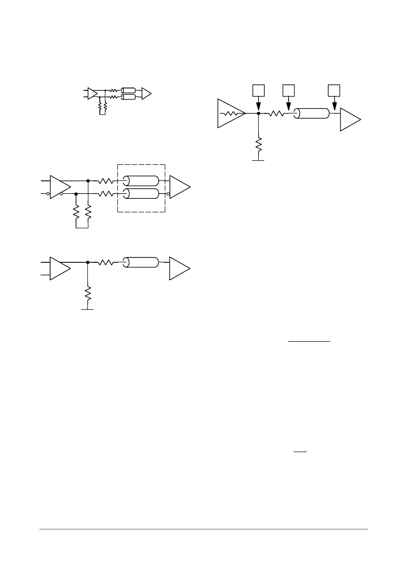
SECTION 4. SERIES TERMINATION
R
R
R
R
Series Damping is a technique in which a termination
resistance is placed between the driver and the transmission
line with no termination resistance placed at the receiving
end of the line (Figure 13).
*TLine Z
0
*TLine Z
0
*TLine Z
0
Driver
R
t
V
EE
R
S
R
S
* Optional
Receiver
Driver
V
EE
R
S
* Optional
Receiver
Figure 13. Series Termination
or Twisted Pair
R
t
R
t
Differential ECL outputs can be terminated as
independent complimentary singleended lines. Both sides
of any differential pair must be terminated as identically as
possible to minimize phase error and pulse width duty cycle
skew.
Series Termination is a special case of series damping in
which the sum of the termination resistor (R
S
) and the output
impedance of the Driver gate (R
O
) is equal to the line
characteristic impedance (Figure 14).
RS
RO
Where:
Z0
(eq. 28)
R
S
= Series Termination Resistor
R
O
= Output Impedance
Z
0
= Line Characteristic Impedance
*TLine Z
0
V
EE
R
S
Receiver
Figure 14. Series Termination
Driver
V
O
A
B
R
O
R
t
Series termination techniques are useful when the
interconnect lengths are long or impedance discontinuities
exist on the line. Additionally, the signal travels down the
line at half amplitude minimizing problems associated with
crosstalk. Unfortunately, a drawback with this technique is
the possibility of a twostep signal appearing when the
driven inputs are far from the end of the transmission line.
To avoid this problem, the distance between the end of the
transmission line and input gates should adhere to the
guidelines specified from the section on unterminated lines.
Series Termination Theory
When the output of the series terminated driver gate
switches levels, this driver output voltage change, V
O
, is
impressed on the input to the transmission line (Point A) as
a change in voltage ( V
A
) and propagates to the Receiver at
the output of the transmission line (Point B) as a change in
voltage ( V
B
) in Figure 14.
VA
VO*
Z0
RO
RS
Z0
(eq. 29)
Where:
V
A
= Input to the Transmission Line Voltage
Change
V
B
= Receiver Input Voltage Change
V
O
= Driver Output Voltage Change
Z
0
= Line Characteristic Impedance
R
O
= Output Impedance of the Driver Gate
R
S
= Termination Resistance
Since Z
0
= R
S
+ R
O
, substitution into the above equations
yields:
VA
VO
2
(eq. 30)
相關(guān)PDF資料 |
PDF描述 |
|---|---|
| AND8020D | Termination of ECL Logic Devices with EF (Emitter Follower) OUTPUT Structure |
| ANP-C-115 | JT 79C 79#22D PIN RECP |
| ANPC-185 | GPS Antenna for Automotive Aftermarket Applications |
| AO3400 | N-Channel Enhancement Mode Field Effect Transistor |
| AO3400L | N-Channel Enhancement Mode Field Effect Transistor |
相關(guān)代理商/技術(shù)參數(shù) |
參數(shù)描述 |
|---|---|
| AND8020D | 制造商:AD 制造商全稱:Analog Devices 功能描述:Termination of ECL Logic Devices with EF (Emitter Follower) OUTPUT Structure |
| AND8028 | 制造商:ONSEMI 制造商全稱:ON Semiconductor 功能描述:Precision Sub-One Volt 1.7 Ampere Output LDO |
| AND8028D | 制造商:ONSEMI 制造商全稱:ON Semiconductor 功能描述:Precision Sub-One Volt 1.7 Ampere Output LDO |
| AND8031 | 制造商:ONSEMI 制造商全稱:ON Semiconductor 功能描述:Isolated Precision Regulation of a Single 1.8 Volt Output from a Universal Line Input |
| AND8031D | 制造商:ONSEMI 制造商全稱:ON Semiconductor 功能描述:Isolated Precision Regulation of a Single 1.8 Volt Output from a Universal Line Input |
發(fā)布緊急采購,3分鐘左右您將得到回復(fù)。