- 您現(xiàn)在的位置:買賣IC網(wǎng) > PDF目錄374016 > ADMC401-PB (Analog Devices, Inc.) Single-Chip, DSP-Based High Performance Motor Controller PDF資料下載
參數(shù)資料
| 型號(hào): | ADMC401-PB |
| 廠商: | Analog Devices, Inc. |
| 英文描述: | Single-Chip, DSP-Based High Performance Motor Controller |
| 中文描述: | 單芯片,基于DSP的高性能電機(jī)控制器 |
| 文件頁(yè)數(shù): | 19/60頁(yè) |
| 文件大?。?/td> | 417K |
| 代理商: | ADMC401-PB |
第1頁(yè)第2頁(yè)第3頁(yè)第4頁(yè)第5頁(yè)第6頁(yè)第7頁(yè)第8頁(yè)第9頁(yè)第10頁(yè)第11頁(yè)第12頁(yè)第13頁(yè)第14頁(yè)第15頁(yè)第16頁(yè)第17頁(yè)第18頁(yè)當(dāng)前第19頁(yè)第20頁(yè)第21頁(yè)第22頁(yè)第23頁(yè)第24頁(yè)第25頁(yè)第26頁(yè)第27頁(yè)第28頁(yè)第29頁(yè)第30頁(yè)第31頁(yè)第32頁(yè)第33頁(yè)第34頁(yè)第35頁(yè)第36頁(yè)第37頁(yè)第38頁(yè)第39頁(yè)第40頁(yè)第41頁(yè)第42頁(yè)第43頁(yè)第44頁(yè)第45頁(yè)第46頁(yè)第47頁(yè)第48頁(yè)第49頁(yè)第50頁(yè)第51頁(yè)第52頁(yè)第53頁(yè)第54頁(yè)第55頁(yè)第56頁(yè)第57頁(yè)第58頁(yè)第59頁(yè)第60頁(yè)
ADMC401
–19–
REV. B
SYSTEM INTERFACE
CLOCK SIGNALS
The ADMC401 uses an input clock with a frequency equal to
half the instruction rate; a 13 MHz input clock yields a 38.5 ns
processor cycle (which is equivalent to 26 MHz). Normally
instructions are executed in a single processor cycle. All device
timing is relative to the internal instruction rate, which is indi-
cated by the CLKOUT signal (when enabled). Throughout this
data sheet, the period of the CLKIN signal is denoted by t
CKI
.
The DSP instruction period is t
CK
(the period of the CLKOUT
signal), and t
CK
= 0.5
×
t
CKI
. For 26 MIPS operation, a 13 MHz
CLKIN signal is used, corresponding to t
CKI
= 76.9 ns and t
CK
= 38.5 ns. Additionally, t
CK
is the fundamental time increment
of the motor control peripherals. Therefore, unless otherwise
specified, the motor control peripherals are clocked at a rate
equal to CLKOUT. The ADMC401 can be clocked by either a
crystal or by an external clock source. The CLKIN input cannot
be halted, changed in frequency, or operated below the specified
minimum frequency during normal operation.
If an external clock source is used, it should be a TTL-compatible
signal running at half the instruction rate. The signal is con-
nected to the CLKIN pin of the ADMC401. In this mode, with
an external clock signal, the XTAL pin must be left unconnected.
Because the ADMC401 includes an on-chip oscillator circuit,
an external crystal may be used instead of a clock source. The
crystal should be connected across the CLKIN and XTAL pins.
A parallel-resonant, fundamental frequency, microprocessor-
grade crystal should be used. The frequency value selected for
the crystal should be equal to half the desired instruction rate
for the processor. Figure 15 shows a 13 MHz crystal properly
connected to yield a 26 MHz processor rate.
The CLKOUT output can be enabled and disabled by the
CLKODIS bit of the SPORT0 Autobuffer Control Register,
DM (0x3FF3). However, extreme care must be exercised when
using this bit (and is thus discouraged) since disabling CLKOUT
effectively disables all motor control peripherals, except the
watchdog timer.
RESET AND POWER-ON RESET CIRCUIT
The
RESET
pin initiates a complete hardware reset of the
ADMC401 when pulled low. The
RESET
signal must be asserted
when the device is powered up to assure proper initialization.
The ADMC401 contains an integrated power-on reset circuit
that provides an output reset signal,
POR
, from the ADMC401
on power up and if the power supply voltage falls below the
threshold level. The ADMC401 may be reset from an external
source using the
RESET
signal or alternatively the internal
power-on reset circuit may be used by connecting the
POR
pin
to the
RESET
pin. During power-up the
RESET
line must be
activated for long enough to allow the DSP core’s internal clock
to stabilize. The power-up sequence is defined as the total time
required for the crystal oscillator to stabilize after a valid V
DD
is
applied to the processor and for the internal phase locked loop
(PLL) to lock onto the specific crystal frequency. A minimum of
2000t
CKI
cycles will ensure that the PLL has locked (this does not
include the crystal oscillator start-up time).
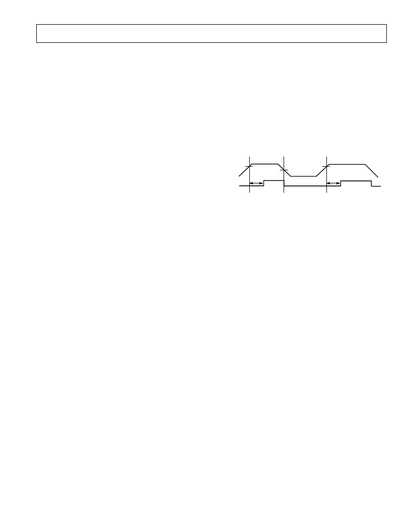
The operation of the internal power-on reset circuit is illustrated
in Figure 14. On power-up, the circuit maintains the
POR
pin
low until it detects that the V
DD
line has attained the threshold
voltage, V
RST
level. As soon as the threshold voltage is attained,
the power on reset circuit enables a 17-bit counter that is
clocked at the CLKOUT rate. While the counter is counting the
POR
pin is held low. When the counter overflows, after a time:
t
ms
RST
=
×
×
=
2
38 5
10
2 52
.
16
9
.
–
the
POR
pin is brought high and if the
POR
and
RESET
pins
are connected, the device is brought out of reset.
The internal power-on reset circuit also acts as a power supply
monitor and puts the
POR
pin at a LO level if it detects a volt-
age less than V
RST
–V
HYST
, where V
HYST
is the hysteresis voltage
built into the POR circuit. The supply voltage must then exceed
V
RST
to initiate another power-on reset sequence.
VDD
POR
t
RST
t
RST
V
RST
V
RST
- V
HYST
Figure 14. Operation of Power-On Reset (POR) Circuit of
ADMC401
The master reset (
RESET
= LO) causes a Full System Reset,
which sets all internal stack pointers to the empty stack condi-
tion, masks all interrupts, clears the MSTAT register, restores
the program counter to its initial value and performs a full reset
of all of the motor control peripherals including the watchdog
timer. Following a power-up, it is possible to initiate a Full
System Reset by simply pulling the
RESET
low. For these
resets, there is no need to wait for PLL stabilization and the
RESET
signal must meet the minimum pulsewidth specifica-
tion, t
RSP
. To generate the external
RESET
signal, it is recom-
mended to use either an RC circuit with a Schmitt trigger or a
commercially available reset IC.
Separate from a Full System Reset, a software controlled Periph-
eral Reset (excluding the watchdog timer) is achieved by toggling
the DSP FL2 flag with the following code segment:
PRESET:
SET FL2;
TOGGLE FL2;
TOGGLE FL2;
RTS;
A full DSP and peripheral reset (except the watchdog timer
itself) will occur automatically on a watchdog trip.
EXTERNAL MEMORY INTERFACE
The ADMC401 can address 14K
×
24 bits of external program
memory and up to 13K
×
16 bits of external data memory. The
ADMC401 provides the address on a 14-bit address bus
(A13–A0). Instructions or data are transferred across the 24-bit
data bus (D23–D0) during program memory accesses. During
data memory accesses, data is transferred on the 16 most signifi-
cant bits (D23–D8) of the data bus. For a dual off-chip fetch,
the data from program memory is read first, then the data from
data memory. The program memory select pin,
PMS
, is acti-
vated during external program memory accesses and can be
used as a chip select signal for the external program memory
devices. Similarly, for external data memory accesses, the
DMS
pin is activated.
相關(guān)PDF資料 |
PDF描述 |
|---|---|
| ADMCF340 | DashDSPTM 64-Lead Flash Mixed-Signal DSP with Enhanced Analog Front End |
| ADMCF340BST | DashDSPTM 64-Lead Flash Mixed-Signal DSP with Enhanced Analog Front End |
| ADMCF340-EVALKIT | Circular Connector; No. of Contacts:7; Series:MS27497; Body Material:Aluminum; Connecting Termination:Crimp; Connector Shell Size:10; Circular Contact Gender:Pin; Circular Shell Style:Wall Mount Receptacle; Insert Arrangement:10-99 RoHS Compliant: No |
| ADMCF341 | DashDSP⑩ 28-Lead Flash Mixed-Signal DSP with Enhanced Analog Front End |
| ADMCF341BR | DashDSP⑩ 28-Lead Flash Mixed-Signal DSP with Enhanced Analog Front End |
相關(guān)代理商/技術(shù)參數(shù) |
參數(shù)描述 |
|---|---|
| ADMCF326 | 制造商:AD 制造商全稱:Analog Devices 功能描述:28-Lead Flash Memory DSP Motor Controller |
| ADMCF326BN | 制造商:Analog Devices 功能描述: |
| ADMCF326BR | 制造商:AD 制造商全稱:Analog Devices 功能描述:28-Lead Flash Memory DSP Motor Controller |
| ADMCF326BRZ | 制造商:Rochester Electronics LLC 功能描述: 制造商:Analog Devices 功能描述: |
| ADMCF326BRZ-REEL | 制造商:Rochester Electronics LLC 功能描述: 制造商:Analog Devices 功能描述: |
發(fā)布緊急采購(gòu),3分鐘左右您將得到回復(fù)。