- 您現(xiàn)在的位置:買賣IC網(wǎng) > PDF目錄11767 > AD6620ASZ-REEL (Analog Devices Inc)IC DGTL RCVR DUAL 67MSPS 80-PQFP PDF資料下載
參數(shù)資料
| 型號(hào): | AD6620ASZ-REEL |
| 廠商: | Analog Devices Inc |
| 文件頁數(shù): | 33/44頁 |
| 文件大?。?/td> | 0K |
| 描述: | IC DGTL RCVR DUAL 67MSPS 80-PQFP |
| 標(biāo)準(zhǔn)包裝: | 500 |
| 接口: | 并行/串行 |
| 電源電壓: | 3 V ~ 3.6 V |
| 封裝/外殼: | 80-BQFP |
| 供應(yīng)商設(shè)備封裝: | 80-PQFP(14x14) |
| 包裝: | 帶卷 (TR) |
| 安裝類型: | 表面貼裝 |
第1頁第2頁第3頁第4頁第5頁第6頁第7頁第8頁第9頁第10頁第11頁第12頁第13頁第14頁第15頁第16頁第17頁第18頁第19頁第20頁第21頁第22頁第23頁第24頁第25頁第26頁第27頁第28頁第29頁第30頁第31頁第32頁當(dāng)前第33頁第34頁第35頁第36頁第37頁第38頁第39頁第40頁第41頁第42頁第43頁第44頁
AD6620
–39–
REV. A
the SDO of the master AD6620 takes control of the SDO line
and begins shifting data out of the device. When all data has
been shifted, the master raises the SDFE on the last shifted.
This signals the next chip (slave) that on the next cycle of the
clock it should take control of the SDO line and begin shifting
data to the DSP. When the second AD6620 completes its shift,
it raises its SDFE to signal the next chip in the chain, if present.
If additional devices are connected to the chain, this would be
used to indicate they should take control on the next clock cycle.
This application does not have a third device and therefore, the
frame would end.
Normally in an application with a single AD6620, the AD6620
would be configured as the serial bus master. However, there
are applications where the DSP or other device may be the serial
bus master. In this case, the diagram below illustrates how to
configure the AD6620 so that it may be used in this mode. In
order to use this in a meaningful application, the DSP must
know when the AD6620 has new data available on its output. If
the DSP polls the AD6620 too early, either old data will be present
or the data could be in an indeterminate state. To prevent this,
the AD6620 has an output pin DVOUT that signals the DSP
when new data is available. This should be tied to an interrupt
line of the DSP that is edge-sensitive, as the DVOUT line is only
valid for two or four high speed clock cycles depending on the
mode of the chip. The DSP may then invoke an interrupt service
routine to handle the data, see text below. In this application,
the DSP is responsible for generating the framing and clocking
signals to the AD6620 as shown in Figure 51.
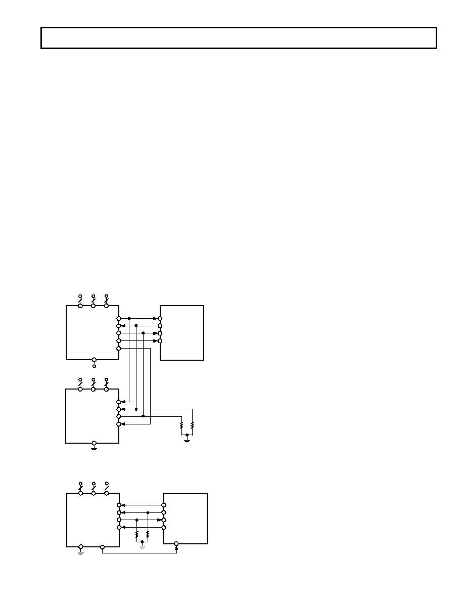
SCLK
AD6620
DSP
+3.3V
SBM
SCLK
SDI
DT
SDO
DR
SDFS
RFS
SDFE
10k
SDIV
2
4
AD
WL
10k
SCLK
SBM
SDI
SDO
SDFS
SDFE
SDIV
2
4
AD
WL
AD6620
CASCADE
Figure 50. Dual AD6620s Using the Serial Bus in a TDM
Application
SCLK
AD6620
DSP
SCLK
SDI
DT
SDO
DR
SDFS
RFS
SDFE
10k
SDIV
2
4
AD
WL
10k
SBM
DVOUT
IRQ
Figure 51. AD6620 Configured as a Serial Slave
Software for Single Channel Real Operation
When interfacing Analog Device’s SHARC DSP, the following
code fragments can be used to configure the SHARC. The first
example shows how to configure the registers for use with a single
channel application. The first segment of code defines the memory
for use with the multichannel serial port data. The second segment
of code sets up the serial port for receiving data only. It could
have just as easily been set up for bidirectional data by properly
setting the MTCSI register. The final two code segments are used
when a serial port interrupt occurs. When the SHARC detects
completion of the serial port frame, an interrupt is generated
and the final code segment is executed. The comments in that
section show where user code should be inserted. The SHARC
takes care of moving the serial port buffers data directly to data
memory as shown.
/
* —————————————————————————————*/
/
* multi-channel register setup */
.SEGMENT/DM dm_data;
.VAR fm_demod_data[2];
/
* Array for receiving 1 real and imag
sample
*/
.VAR fm_demod_tcb[8] = 0, 0, 0, 0, fm_demod_data+7, 2, 1,
fm_demod_data;
/
* Transfer Control Block for reception of fm data */
/
* —————————————————————————————*/
/
* —————————————————————————————*/
/
* Subroutine to setup sport1 for use with the AD6620 */
setup_sport1:
r0 = 0;
/
* multi-channel enable setup */
dm(MTCS1) = r0;
/
* do not transmit on any channels */
r0 = 0;
/
* Compand Setup */
dm(MTCCS1) = r0;
/
* no companding on transmit */
dm(MRCCS1) = r0;
/
* no companding on receive */
r0 = 0x00100000;
/
* Setup sport 1 transmit control register */
dm(STCTL1) = r0;
/
* mfd = 1 */
r0 = 0x038c20f2;
/
* Setup sport 1 receive control register */
dm(SRCTL1) = r0;
/
* slen = 15, sden & schen enabled */
/
* sign extend, external SCLK+RFS */
r0 = fm_demod_tcb + 7; /
* TCB address */
dm(CP1) = r0;
/
* Kickoff DMA chain */
rts (db);
/
* RETURN */
bit set imask SPR1I;
/
* enable sport1 receive interrupt */
nop;
/
* —————————————————————————————*/
spr1_svc:
jump spr1_asserted;
RTI;
/
* —————————————————————————————*/
/
* —————————————————————————————*/
/
* Process received data here. Data samples located in fm_demod_data
and fm_demod_data+1
spr1_asserted:
push sts;
/
* Push the status stack */
/
* Use secondary set of DAGs and Register file */
相關(guān)PDF資料 |
PDF描述 |
|---|---|
| 6274291-2 | CONN JACK VERT PCB 75 OHM BNC |
| AD7669JNZ | IC I/O PORT 8BIT ANLG 28DIP |
| D38999/24FF11PA | CONN RCPT 11POS JAM NUT W/PINS |
| D38999/20JE26HN | CONN RCPT 26POS WALL MNT W/PINS |
| AD7569KNZ | IC I/O PORT 8BIT ANALOG 24DIP |
相關(guān)代理商/技術(shù)參數(shù) |
參數(shù)描述 |
|---|---|
| AD6620PCB | 制造商:AD 制造商全稱:Analog Devices 功能描述:65 MSPS Digital Receive Signal Processor |
| AD6620S | 制造商:AD 制造商全稱:Analog Devices 功能描述:65 MSPS Digital Receive Signal Processor |
| AD6620S/PCB | 制造商:Analog Devices 功能描述:DUAL CHANNEL DECIMATING RECEIV 制造商:Analog Devices 功能描述:SGNL PROCESSOR 169CSPBGA - Bulk |
| AD6622 | 制造商:AD 制造商全稱:Analog Devices 功能描述:Four-Channel, 75 MSPS Digital Transmit Signal Processor TSP |
| AD6622AS | 制造商:Analog Devices 功能描述:Transmit Signal Processor 128-Pin MQFP 制造商:Rochester Electronics LLC 功能描述:4 CHANNEL 65 MSPS DIGITAL UPCONVERTER - Bulk |
發(fā)布緊急采購,3分鐘左右您將得到回復(fù)。