- 您現(xiàn)在的位置:買賣IC網(wǎng) > PDF目錄384066 > μPD78196Y (NEC Corp.) 8 Bit Single Chip Microcontrollers(8 位單片微控制器) PDF資料下載
參數(shù)資料
| 型號: | μPD78196Y |
| 廠商: | NEC Corp. |
| 英文描述: | 8 Bit Single Chip Microcontrollers(8 位單片微控制器) |
| 中文描述: | 8位單片機微控制器(8位單片微控制器) |
| 文件頁數(shù): | 48/365頁 |
| 文件大?。?/td> | 1416K |
| 代理商: | ΜPD78196Y |
第1頁第2頁第3頁第4頁第5頁第6頁第7頁第8頁第9頁第10頁第11頁第12頁第13頁第14頁第15頁第16頁第17頁第18頁第19頁第20頁第21頁第22頁第23頁第24頁第25頁第26頁第27頁第28頁第29頁第30頁第31頁第32頁第33頁第34頁第35頁第36頁第37頁第38頁第39頁第40頁第41頁第42頁第43頁第44頁第45頁第46頁第47頁當(dāng)前第48頁第49頁第50頁第51頁第52頁第53頁第54頁第55頁第56頁第57頁第58頁第59頁第60頁第61頁第62頁第63頁第64頁第65頁第66頁第67頁第68頁第69頁第70頁第71頁第72頁第73頁第74頁第75頁第76頁第77頁第78頁第79頁第80頁第81頁第82頁第83頁第84頁第85頁第86頁第87頁第88頁第89頁第90頁第91頁第92頁第93頁第94頁第95頁第96頁第97頁第98頁第99頁第100頁第101頁第102頁第103頁第104頁第105頁第106頁第107頁第108頁第109頁第110頁第111頁第112頁第113頁第114頁第115頁第116頁第117頁第118頁第119頁第120頁第121頁第122頁第123頁第124頁第125頁第126頁第127頁第128頁第129頁第130頁第131頁第132頁第133頁第134頁第135頁第136頁第137頁第138頁第139頁第140頁第141頁第142頁第143頁第144頁第145頁第146頁第147頁第148頁第149頁第150頁第151頁第152頁第153頁第154頁第155頁第156頁第157頁第158頁第159頁第160頁第161頁第162頁第163頁第164頁第165頁第166頁第167頁第168頁第169頁第170頁第171頁第172頁第173頁第174頁第175頁第176頁第177頁第178頁第179頁第180頁第181頁第182頁第183頁第184頁第185頁第186頁第187頁第188頁第189頁第190頁第191頁第192頁第193頁第194頁第195頁第196頁第197頁第198頁第199頁第200頁第201頁第202頁第203頁第204頁第205頁第206頁第207頁第208頁第209頁第210頁第211頁第212頁第213頁第214頁第215頁第216頁第217頁第218頁第219頁第220頁第221頁第222頁第223頁第224頁第225頁第226頁第227頁第228頁第229頁第230頁第231頁第232頁第233頁第234頁第235頁第236頁第237頁第238頁第239頁第240頁第241頁第242頁第243頁第244頁第245頁第246頁第247頁第248頁第249頁第250頁第251頁第252頁第253頁第254頁第255頁第256頁第257頁第258頁第259頁第260頁第261頁第262頁第263頁第264頁第265頁第266頁第267頁第268頁第269頁第270頁第271頁第272頁第273頁第274頁第275頁第276頁第277頁第278頁第279頁第280頁第281頁第282頁第283頁第284頁第285頁第286頁第287頁第288頁第289頁第290頁第291頁第292頁第293頁第294頁第295頁第296頁第297頁第298頁第299頁第300頁第301頁第302頁第303頁第304頁第305頁第306頁第307頁第308頁第309頁第310頁第311頁第312頁第313頁第314頁第315頁第316頁第317頁第318頁第319頁第320頁第321頁第322頁第323頁第324頁第325頁第326頁第327頁第328頁第329頁第330頁第331頁第332頁第333頁第334頁第335頁第336頁第337頁第338頁第339頁第340頁第341頁第342頁第343頁第344頁第345頁第346頁第347頁第348頁第349頁第350頁第351頁第352頁第353頁第354頁第355頁第356頁第357頁第358頁第359頁第360頁第361頁第362頁第363頁第364頁第365頁
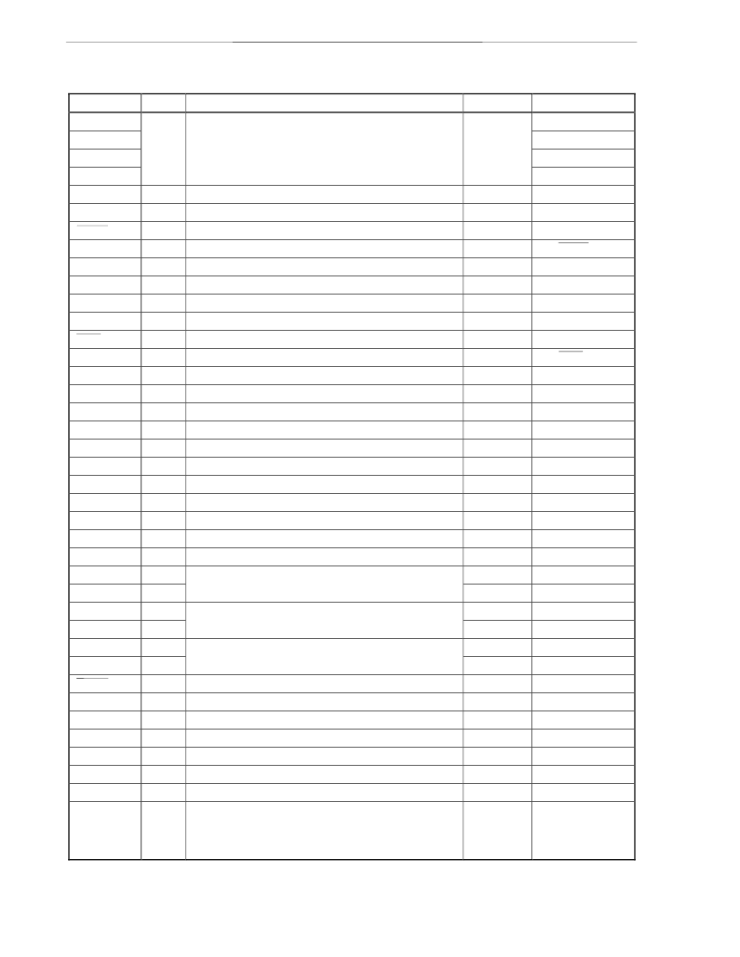
CHAPTER 3 PIN FUNCTIONS
48
(2)
Non-port pins
Pin Name
I/O
Function
After Reset
Alternate Function
INTP0
P30/TI81/CPT90
INTP1
P31/TO81
INTP2
P32/TO90
INTP3
Input
External interrupt input for which effective edges (rising
and/or falling edges) can be specified
Input
P33/TO82/BZO90
SI20
Input
Serial data input to serial interface
Input
P22/RxD20
SO20
Output
Serial data output from serial interface
Input
P21/TxD20
SCK20
I/O
Serial clock input/output for serial interface
Input
P20/ASCK20
ASCK20
Input
Serial clock input to asynchronous serial interface
Input
P20/SCK20
RxD20
Input
Serial data input to asynchronous serial interface
Input
P22/SI20
TxD20
Output
Serial data output from asynchronous serial interface
Input
P21/SO20
SCL0
I/O
SMB0 clock input/output
Input
P23
SDA0
I/O
SMB0 data input/output
Input
P24
SS20
Input
Chip select input to serial interface
Input
P25/TI80
TI80
Input
External count clock input to 8-bit timer (TM80)
Input
P25/SS20
TI81
Input
External count clock input to 8-bit timer (TM81)
Input
P30/INTP0/CPT90
TO80
Output
8-bit timer (TM80) output
Input
P26
TO81
Output
8-bit timer (TM81) output
Input
P31/INTP1
TO82
Output
8-bit timer (TM82) output
Input
P33/INTP3/BZO90
TO90
Output
16-bit timer (TM90) output
Input
P32/INTP2
CPT90
Input
Capture edge input
Input
P30/INTP0/TI81
BZO90
Output
Buzzer output
Input
P33/INTP3/TO82
ANI0 to ANI7
Input
A/D converter analog input
Input
P60 to P67
AV
REF
A/D converter reference voltage
AV
SS
A/D converter ground potential
AV
DD
A/D converter analog power supply
X1
Input
X2
Connected to crystal for main system clock oscillation
CL1
Input
CL2
Connect a resistor (R) and capacitor (C) for main system
clock oscillation
XT1
Input
XT2
Connected to crystal for subsystem clock oscillation
RESET
Input
System reset input
Input
V
DD0
Positive supply voltage for ports
V
DD1
Positive supply voltage for circuits other than ports
V
SS0
Port section ground potential
V
SS1
Ground potential of circuits other than ports
IC0
Internally connect this pin directly to the V
SS0
or V
SS1
pin.
IC2
Internally connect. Leave this pin open.
V
PP
This pin is used to set flash memory programming mode and
applies a high voltage when a program is written or verified.
In normal operation mode, connect this pin directly to the
V
SS0
or V
SS1
pin.
相關(guān)PDF資料 |
PDF描述 |
|---|---|
| μPD78197Y | 8 Bit Single Chip Microcontrollers(8 位單片微控制器) |
| μPD784031(A) | 8/16 Bit Single Chip Microcontrollers(8/16 位單片微控制器) |
| μPD784031Y | 8/16 Bit Single Chip Microcontrollers(8/16 位微控制器) |
| μPD784031 | 8/16 Bit Single Chip Microcontrollers(8/16 位微控制器) |
| μPD784214Y | 8/16 Bit RISC Microcontrollers(8/16位RISC微控制器) |
相關(guān)代理商/技術(shù)參數(shù) |
參數(shù)描述 |
|---|---|
| PD784054GCA2 | 制造商:NEC 制造商全稱:NEC 功能描述:16-BIT SINGLE-CHIP MICROCONTROLLER |
| PD784976A | 制造商:NEC 制造商全稱:NEC 功能描述:16-Bit Single-Chip Microcontroller |
| PD7869 | 制造商:未知廠家 制造商全稱:未知廠家 功能描述:Optoelectronic |
| PD78F0134 | 制造商:NEC 制造商全稱:NEC 功能描述:8-Bit Single-Chip Microcontrollers |
| PD78F0134(A) | 制造商:NEC 制造商全稱:NEC 功能描述:8-Bit Single-Chip Microcontrollers |
發(fā)布緊急采購,3分鐘左右您將得到回復(fù)。