- 您現(xiàn)在的位置:買賣IC網(wǎng) > PDF目錄372925 > XPC755BRX400LE Microprocessor PDF資料下載
參數(shù)資料
| 型號(hào): | XPC755BRX400LE |
| 英文描述: | Microprocessor |
| 中文描述: | 微處理器 |
| 文件頁數(shù): | 35/52頁 |
| 文件大?。?/td> | 1274K |
| 代理商: | XPC755BRX400LE |
第1頁第2頁第3頁第4頁第5頁第6頁第7頁第8頁第9頁第10頁第11頁第12頁第13頁第14頁第15頁第16頁第17頁第18頁第19頁第20頁第21頁第22頁第23頁第24頁第25頁第26頁第27頁第28頁第29頁第30頁第31頁第32頁第33頁第34頁當(dāng)前第35頁第36頁第37頁第38頁第39頁第40頁第41頁第42頁第43頁第44頁第45頁第46頁第47頁第48頁第49頁第50頁第51頁第52頁
MOTOROLA
MPC755 RISC Microprocessor Hardware Specifications
35
System Design Information
1.8.2
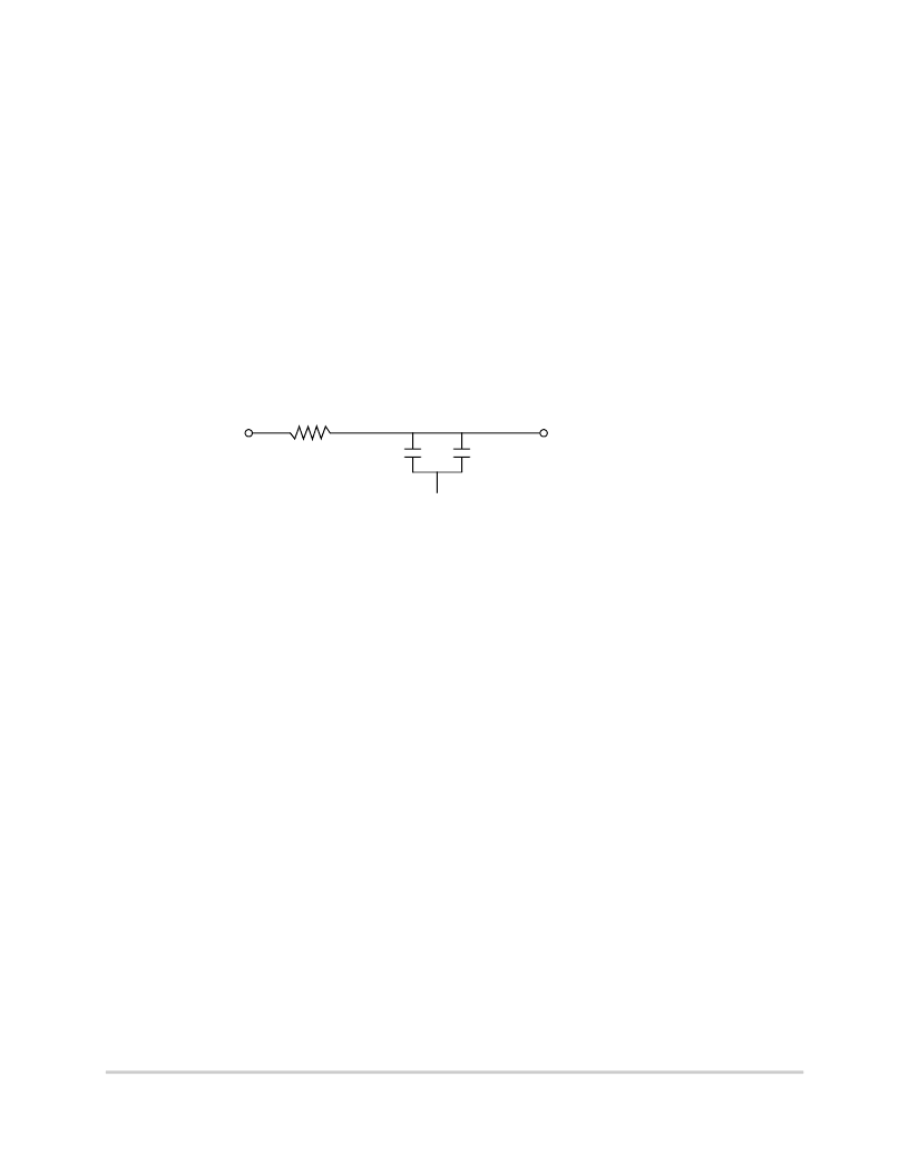
PLL Power Supply Filtering
The AV
DD
and L2AV
DD
power signals are provided on the MPC755 to provide power to the clock
generation PLL and L2 cache DLL, respectively. To ensure stability of the internal clock, the power supplied
to the AV
DD
input signal should be filtered of any noise in the 500 kHz to 10 MHz resonant frequency range
of the PLL. A circuit similar to the one shown in Figure 21 using surface mount capacitors with minimum
Effective Series Inductance (ESL) is recommended. Consistent with the recommendations of Dr. Howard
Johnson in
High Speed Digital Design: A Handbook of Black Magic
(Prentice Hall, 1993), multiple small
capacitors of equal value are recommended over a single large value capacitor.
The circuit should be placed as close as possible to the AV
DD
pin to minimize noise coupled from nearby
circuits. An identical but separate circuit should be placed as close as possible to the L2AV
DD
pin. It is often
possible to route directly from the capacitors to the AV
DD
pin, which is on the periphery of the 360 BGA
footprint, without the inductance of vias. The L2AV
DD
pin may be more difficult to route, but is
proportionately less critical.
FIgure 21 shows the PLL power supply filter circuit.
Figure 21. PLL Power Supply Filter Circuit
1.8.3
Decoupling Recommendations
Due to the MPC755 dynamic power management feature, large address and data buses, and high operating
frequencies, the MPC755 can generate transient power surges and high frequency noise in its power supply,
especially while driving large capacitive loads. This noise must be prevented from reaching other
components in the MPC755 system, and the MPC755 itself requires a clean, tightly regulated source of
power. Therefore, it is recommended that the system designer place at least one decoupling capacitor at each
V
DD
, OV
DD
, and L2OV
DD
pin of the MPC755. It is also recommended that these decoupling capacitors
receive their power from separate V
DD
, (L2)OV
DD
, and GND power planes in the PCB, utilizing short
traces to minimize inductance.
These capacitors should have a value of 0.01 μF or 0.1 μF. Only ceramic SMT (surface mount technology)
capacitors should be used to minimize lead inductance, preferably 0508 or 0603 orientations where
connections are made along the length of the part.
In addition, it is recommended that there be several bulk storage capacitors distributed around the PCB,
feeding the V
DD
, L2OV
DD
, and OV
DD
planes, to enable quick recharging of the smaller chip capacitors.
These bulk capacitors should have a low ESR (equivalent series resistance) rating to ensure the quick
response time necessary. They should also be connected to the power and ground planes through two vias
to minimize inductance. Suggested bulk capacitors:100–330 μF (AVX TPS tantalum or Sanyo OSCON).
1.8.4
Connection Recommendations
To ensure reliable operation, it is highly recommended to connect unused inputs to an appropriate signal
level through a resistor. Unused active low inputs should be tied to OV
DD
. Unused active high inputs should
be connected to GND. All NC (no connect) signals must remain unconnected.
V
DD
AV
DD
(or L2AV
DD
)
10
2.2 μF
2.2 μF
GND
Low ESL Surface Mount Capacitors
相關(guān)PDF資料 |
PDF描述 |
|---|---|
| XPC750EC | XPC750P/D XPC750P RISC Microprocessor Hardware Specifications |
| XPC801ZP25 | Microprocessor |
| XPC801ZP40 | Microprocessor |
| XPC821ZP40 | Microprocessor |
| XPC823ZP25 | Microprocessor |
相關(guān)代理商/技術(shù)參數(shù) |
參數(shù)描述 |
|---|---|
| XPC801ZP25 | 制造商:未知廠家 制造商全稱:未知廠家 功能描述:Microprocessor |
| XPC801ZP40 | 制造商:未知廠家 制造商全稱:未知廠家 功能描述:Microprocessor |
| XPC821ZP40 | 制造商:未知廠家 制造商全稱:未知廠家 功能描述:Microprocessor |
| XPC823CVR66B2T | 功能描述:IC MPU POWERQUICC 66MHZ 256-PBGA RoHS:是 類別:集成電路 (IC) >> 嵌入式 - 微處理器 系列:MPC8xx 標(biāo)準(zhǔn)包裝:2 系列:MPC8xx 處理器類型:32-位 MPC8xx PowerQUICC 特點(diǎn):- 速度:133MHz 電壓:3.3V 安裝類型:表面貼裝 封裝/外殼:357-BBGA 供應(yīng)商設(shè)備封裝:357-PBGA(25x25) 包裝:托盤 |
| XPC823CZC66A | 制造商:Freescale Semiconductor 功能描述: |
發(fā)布緊急采購,3分鐘左右您將得到回復(fù)。