- 您現(xiàn)在的位置:買賣IC網(wǎng) > PDF目錄200646 > UPD789417AGK-XXX-9EU 8-BIT, MROM, 5 MHz, MICROCONTROLLER, PQFP80 PDF資料下載
參數(shù)資料
| 型號(hào): | UPD789417AGK-XXX-9EU |
| 元件分類: | 微控制器/微處理器 |
| 英文描述: | 8-BIT, MROM, 5 MHz, MICROCONTROLLER, PQFP80 |
| 封裝: | 12 X 12 MM, PLASTIC, TQFP-80 |
| 文件頁(yè)數(shù): | 183/320頁(yè) |
| 文件大?。?/td> | 2550K |
| 代理商: | UPD789417AGK-XXX-9EU |
第1頁(yè)第2頁(yè)第3頁(yè)第4頁(yè)第5頁(yè)第6頁(yè)第7頁(yè)第8頁(yè)第9頁(yè)第10頁(yè)第11頁(yè)第12頁(yè)第13頁(yè)第14頁(yè)第15頁(yè)第16頁(yè)第17頁(yè)第18頁(yè)第19頁(yè)第20頁(yè)第21頁(yè)第22頁(yè)第23頁(yè)第24頁(yè)第25頁(yè)第26頁(yè)第27頁(yè)第28頁(yè)第29頁(yè)第30頁(yè)第31頁(yè)第32頁(yè)第33頁(yè)第34頁(yè)第35頁(yè)第36頁(yè)第37頁(yè)第38頁(yè)第39頁(yè)第40頁(yè)第41頁(yè)第42頁(yè)第43頁(yè)第44頁(yè)第45頁(yè)第46頁(yè)第47頁(yè)第48頁(yè)第49頁(yè)第50頁(yè)第51頁(yè)第52頁(yè)第53頁(yè)第54頁(yè)第55頁(yè)第56頁(yè)第57頁(yè)第58頁(yè)第59頁(yè)第60頁(yè)第61頁(yè)第62頁(yè)第63頁(yè)第64頁(yè)第65頁(yè)第66頁(yè)第67頁(yè)第68頁(yè)第69頁(yè)第70頁(yè)第71頁(yè)第72頁(yè)第73頁(yè)第74頁(yè)第75頁(yè)第76頁(yè)第77頁(yè)第78頁(yè)第79頁(yè)第80頁(yè)第81頁(yè)第82頁(yè)第83頁(yè)第84頁(yè)第85頁(yè)第86頁(yè)第87頁(yè)第88頁(yè)第89頁(yè)第90頁(yè)第91頁(yè)第92頁(yè)第93頁(yè)第94頁(yè)第95頁(yè)第96頁(yè)第97頁(yè)第98頁(yè)第99頁(yè)第100頁(yè)第101頁(yè)第102頁(yè)第103頁(yè)第104頁(yè)第105頁(yè)第106頁(yè)第107頁(yè)第108頁(yè)第109頁(yè)第110頁(yè)第111頁(yè)第112頁(yè)第113頁(yè)第114頁(yè)第115頁(yè)第116頁(yè)第117頁(yè)第118頁(yè)第119頁(yè)第120頁(yè)第121頁(yè)第122頁(yè)第123頁(yè)第124頁(yè)第125頁(yè)第126頁(yè)第127頁(yè)第128頁(yè)第129頁(yè)第130頁(yè)第131頁(yè)第132頁(yè)第133頁(yè)第134頁(yè)第135頁(yè)第136頁(yè)第137頁(yè)第138頁(yè)第139頁(yè)第140頁(yè)第141頁(yè)第142頁(yè)第143頁(yè)第144頁(yè)第145頁(yè)第146頁(yè)第147頁(yè)第148頁(yè)第149頁(yè)第150頁(yè)第151頁(yè)第152頁(yè)第153頁(yè)第154頁(yè)第155頁(yè)第156頁(yè)第157頁(yè)第158頁(yè)第159頁(yè)第160頁(yè)第161頁(yè)第162頁(yè)第163頁(yè)第164頁(yè)第165頁(yè)第166頁(yè)第167頁(yè)第168頁(yè)第169頁(yè)第170頁(yè)第171頁(yè)第172頁(yè)第173頁(yè)第174頁(yè)第175頁(yè)第176頁(yè)第177頁(yè)第178頁(yè)第179頁(yè)第180頁(yè)第181頁(yè)第182頁(yè)當(dāng)前第183頁(yè)第184頁(yè)第185頁(yè)第186頁(yè)第187頁(yè)第188頁(yè)第189頁(yè)第190頁(yè)第191頁(yè)第192頁(yè)第193頁(yè)第194頁(yè)第195頁(yè)第196頁(yè)第197頁(yè)第198頁(yè)第199頁(yè)第200頁(yè)第201頁(yè)第202頁(yè)第203頁(yè)第204頁(yè)第205頁(yè)第206頁(yè)第207頁(yè)第208頁(yè)第209頁(yè)第210頁(yè)第211頁(yè)第212頁(yè)第213頁(yè)第214頁(yè)第215頁(yè)第216頁(yè)第217頁(yè)第218頁(yè)第219頁(yè)第220頁(yè)第221頁(yè)第222頁(yè)第223頁(yè)第224頁(yè)第225頁(yè)第226頁(yè)第227頁(yè)第228頁(yè)第229頁(yè)第230頁(yè)第231頁(yè)第232頁(yè)第233頁(yè)第234頁(yè)第235頁(yè)第236頁(yè)第237頁(yè)第238頁(yè)第239頁(yè)第240頁(yè)第241頁(yè)第242頁(yè)第243頁(yè)第244頁(yè)第245頁(yè)第246頁(yè)第247頁(yè)第248頁(yè)第249頁(yè)第250頁(yè)第251頁(yè)第252頁(yè)第253頁(yè)第254頁(yè)第255頁(yè)第256頁(yè)第257頁(yè)第258頁(yè)第259頁(yè)第260頁(yè)第261頁(yè)第262頁(yè)第263頁(yè)第264頁(yè)第265頁(yè)第266頁(yè)第267頁(yè)第268頁(yè)第269頁(yè)第270頁(yè)第271頁(yè)第272頁(yè)第273頁(yè)第274頁(yè)第275頁(yè)第276頁(yè)第277頁(yè)第278頁(yè)第279頁(yè)第280頁(yè)第281頁(yè)第282頁(yè)第283頁(yè)第284頁(yè)第285頁(yè)第286頁(yè)第287頁(yè)第288頁(yè)第289頁(yè)第290頁(yè)第291頁(yè)第292頁(yè)第293頁(yè)第294頁(yè)第295頁(yè)第296頁(yè)第297頁(yè)第298頁(yè)第299頁(yè)第300頁(yè)第301頁(yè)第302頁(yè)第303頁(yè)第304頁(yè)第305頁(yè)第306頁(yè)第307頁(yè)第308頁(yè)第309頁(yè)第310頁(yè)第311頁(yè)第312頁(yè)第313頁(yè)第314頁(yè)第315頁(yè)第316頁(yè)第317頁(yè)第318頁(yè)第319頁(yè)第320頁(yè)
CHAPTER 18
PD78F9418A
User’s Manual U13952EJ3V1UD
263
<RESET pin>
When the reset signal of the dedicated flash programmer is connected to the RESET pin connected to the reset
signal generator on the board, a signal conflict occurs. To prevent this signal conflict, isolate the connection with
the reset signal generator.
If a reset signal is input from the user system in the flash memory programming mode, a normal programming
operation will not be performed. Do not input signals other than reset signals from the dedicated flash programmer
during this period.
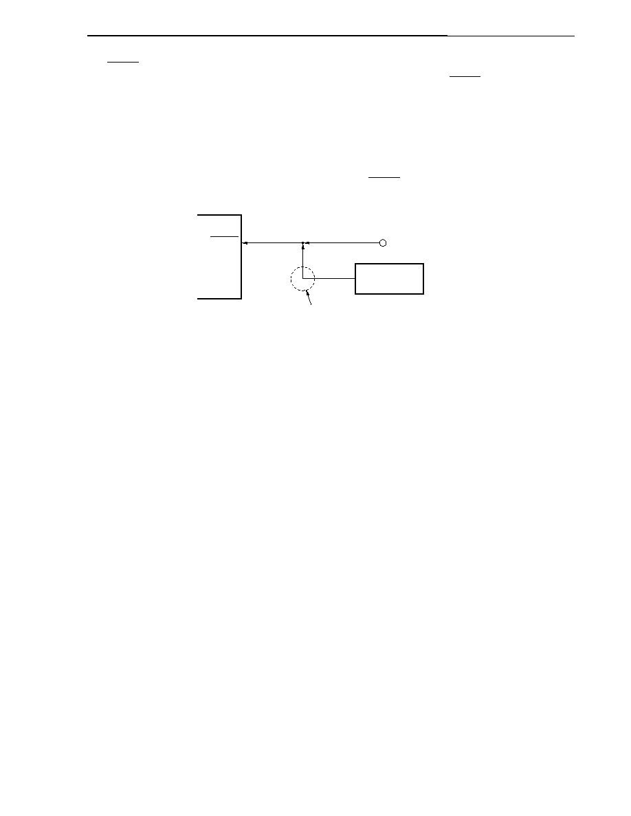
Figure 18-7. Signal Conflict (RESET Pin)
RESET
PD78F9418A
Signal conflict
Output pin
Reset signal generator
In the flash memory programming mode, the signal output
by the reset signal generator and the signal output by the
dedicated flash programmer conflict, therefore, isolate the
signal on the reset signal generator side.
Connection pin of dedicated
flash programmer
<Port pins>
Shifting to the flash memory programming mode sets all the pins except those used for flash memory
programming communication to the status immediately after reset.
Therefore, if the external device does not acknowledge an initial status such as the output high impedance
status, connect the external device to VDD0, VDD1, VSS0, or VSS1 via a resistor.
<Oscillation pins>
When using an on-board clock, connection of X1, X2, XT1, and XT2 must conform to the methods in the normal
operation mode.
When using the clock output of the flash programmer, directly connect it to the X1 pin with the on-board main
oscillator disconnected, and leave the X2 pin open. For the subclock, connection conforms to that in the normal
operation mode.
<Power supply>
To use the power output of the flash programmer, connect the VDD0 and VDD1 pins to VDD of the flash
programmer, and the VSS0 and VSS1 pins to GND of the flash programmer.
To use the on-board power supply, connection must conform to that in the normal operation mode. However,
because the voltage is monitored by the flash programmer, therefore, VDD of the flash programmer must be
connected.
For the other power supply pins (AVDD, AVREF, AVSS), supply the same power supply as in the normal operation
mode.
<Other pins>
Handle the other pins (S0 to S15, COM0 to COM3, VLC0 to VLC2, BIAS) in the same way as in the normal
operation mode.
相關(guān)PDF資料 |
PDF描述 |
|---|---|
| UPD78F0361GB(R)-UEU-A | 8-BIT, FLASH, 20 MHz, MICROCONTROLLER, PQFP64 |
| UPD78F0361GB(T)-UEU-A | 8-BIT, FLASH, 20 MHz, MICROCONTROLLER, PQFP64 |
| UPD78F0361GK(R)-UET-A | 8-BIT, FLASH, 20 MHz, MICROCONTROLLER, PQFP64 |
| UPD78F0361GK(S)-UET-A | 8-BIT, FLASH, 20 MHz, MICROCONTROLLER, PQFP64 |
| UPD78F0397GC(S)-8EU-A | 8-BIT, FLASH, 20 MHz, MICROCONTROLLER, PQFP100 |
相關(guān)代理商/技術(shù)參數(shù) |
參數(shù)描述 |
|---|---|
| UPD789445GB-8EU-A | 制造商:Renesas Electronics Corporation 功能描述: |
| UPD789488GK-517-9EU | 制造商:NEC Electronics Corporation 功能描述: |
| UPD789850MC(A)-028-5A4 | 制造商:Renesas Electronics Corporation 功能描述: |
| UPD789850MC(A)-028-5A4-A | 制造商:Renesas Electronics Corporation 功能描述: |
| UPD78C10ACW | 制造商:NEC Electronics Corporation 功能描述: |
發(fā)布緊急采購(gòu),3分鐘左右您將得到回復(fù)。