- 您現(xiàn)在的位置:買賣IC網(wǎng) > PDF目錄371187 > TMXF28155 TMXF28155 Super Mapper 155/51 Mbits/s SONET/SDH x28/x21 DS1/E1 PDF資料下載
參數(shù)資料
| 型號(hào): | TMXF28155 |
| 英文描述: | TMXF28155 Super Mapper 155/51 Mbits/s SONET/SDH x28/x21 DS1/E1 |
| 中文描述: | TMXF28155超級(jí)映射五十一分之一百五十五Mbits /秒的SONET / SDH x28/x21的DS1/E1 |
| 文件頁數(shù): | 273/606頁 |
| 文件大小: | 9520K |
| 代理商: | TMXF28155 |
第1頁第2頁第3頁第4頁第5頁第6頁第7頁第8頁第9頁第10頁第11頁第12頁第13頁第14頁第15頁第16頁第17頁第18頁第19頁第20頁第21頁第22頁第23頁第24頁第25頁第26頁第27頁第28頁第29頁第30頁第31頁第32頁第33頁第34頁第35頁第36頁第37頁第38頁第39頁第40頁第41頁第42頁第43頁第44頁第45頁第46頁第47頁第48頁第49頁第50頁第51頁第52頁第53頁第54頁第55頁第56頁第57頁第58頁第59頁第60頁第61頁第62頁第63頁第64頁第65頁第66頁第67頁第68頁第69頁第70頁第71頁第72頁第73頁第74頁第75頁第76頁第77頁第78頁第79頁第80頁第81頁第82頁第83頁第84頁第85頁第86頁第87頁第88頁第89頁第90頁第91頁第92頁第93頁第94頁第95頁第96頁第97頁第98頁第99頁第100頁第101頁第102頁第103頁第104頁第105頁第106頁第107頁第108頁第109頁第110頁第111頁第112頁第113頁第114頁第115頁第116頁第117頁第118頁第119頁第120頁第121頁第122頁第123頁第124頁第125頁第126頁第127頁第128頁第129頁第130頁第131頁第132頁第133頁第134頁第135頁第136頁第137頁第138頁第139頁第140頁第141頁第142頁第143頁第144頁第145頁第146頁第147頁第148頁第149頁第150頁第151頁第152頁第153頁第154頁第155頁第156頁第157頁第158頁第159頁第160頁第161頁第162頁第163頁第164頁第165頁第166頁第167頁第168頁第169頁第170頁第171頁第172頁第173頁第174頁第175頁第176頁第177頁第178頁第179頁第180頁第181頁第182頁第183頁第184頁第185頁第186頁第187頁第188頁第189頁第190頁第191頁第192頁第193頁第194頁第195頁第196頁第197頁第198頁第199頁第200頁第201頁第202頁第203頁第204頁第205頁第206頁第207頁第208頁第209頁第210頁第211頁第212頁第213頁第214頁第215頁第216頁第217頁第218頁第219頁第220頁第221頁第222頁第223頁第224頁第225頁第226頁第227頁第228頁第229頁第230頁第231頁第232頁第233頁第234頁第235頁第236頁第237頁第238頁第239頁第240頁第241頁第242頁第243頁第244頁第245頁第246頁第247頁第248頁第249頁第250頁第251頁第252頁第253頁第254頁第255頁第256頁第257頁第258頁第259頁第260頁第261頁第262頁第263頁第264頁第265頁第266頁第267頁第268頁第269頁第270頁第271頁第272頁當(dāng)前第273頁第274頁第275頁第276頁第277頁第278頁第279頁第280頁第281頁第282頁第283頁第284頁第285頁第286頁第287頁第288頁第289頁第290頁第291頁第292頁第293頁第294頁第295頁第296頁第297頁第298頁第299頁第300頁第301頁第302頁第303頁第304頁第305頁第306頁第307頁第308頁第309頁第310頁第311頁第312頁第313頁第314頁第315頁第316頁第317頁第318頁第319頁第320頁第321頁第322頁第323頁第324頁第325頁第326頁第327頁第328頁第329頁第330頁第331頁第332頁第333頁第334頁第335頁第336頁第337頁第338頁第339頁第340頁第341頁第342頁第343頁第344頁第345頁第346頁第347頁第348頁第349頁第350頁第351頁第352頁第353頁第354頁第355頁第356頁第357頁第358頁第359頁第360頁第361頁第362頁第363頁第364頁第365頁第366頁第367頁第368頁第369頁第370頁第371頁第372頁第373頁第374頁第375頁第376頁第377頁第378頁第379頁第380頁第381頁第382頁第383頁第384頁第385頁第386頁第387頁第388頁第389頁第390頁第391頁第392頁第393頁第394頁第395頁第396頁第397頁第398頁第399頁第400頁第401頁第402頁第403頁第404頁第405頁第406頁第407頁第408頁第409頁第410頁第411頁第412頁第413頁第414頁第415頁第416頁第417頁第418頁第419頁第420頁第421頁第422頁第423頁第424頁第425頁第426頁第427頁第428頁第429頁第430頁第431頁第432頁第433頁第434頁第435頁第436頁第437頁第438頁第439頁第440頁第441頁第442頁第443頁第444頁第445頁第446頁第447頁第448頁第449頁第450頁第451頁第452頁第453頁第454頁第455頁第456頁第457頁第458頁第459頁第460頁第461頁第462頁第463頁第464頁第465頁第466頁第467頁第468頁第469頁第470頁第471頁第472頁第473頁第474頁第475頁第476頁第477頁第478頁第479頁第480頁第481頁第482頁第483頁第484頁第485頁第486頁第487頁第488頁第489頁第490頁第491頁第492頁第493頁第494頁第495頁第496頁第497頁第498頁第499頁第500頁第501頁第502頁第503頁第504頁第505頁第506頁第507頁第508頁第509頁第510頁第511頁第512頁第513頁第514頁第515頁第516頁第517頁第518頁第519頁第520頁第521頁第522頁第523頁第524頁第525頁第526頁第527頁第528頁第529頁第530頁第531頁第532頁第533頁第534頁第535頁第536頁第537頁第538頁第539頁第540頁第541頁第542頁第543頁第544頁第545頁第546頁第547頁第548頁第549頁第550頁第551頁第552頁第553頁第554頁第555頁第556頁第557頁第558頁第559頁第560頁第561頁第562頁第563頁第564頁第565頁第566頁第567頁第568頁第569頁第570頁第571頁第572頁第573頁第574頁第575頁第576頁第577頁第578頁第579頁第580頁第581頁第582頁第583頁第584頁第585頁第586頁第587頁第588頁第589頁第590頁第591頁第592頁第593頁第594頁第595頁第596頁第597頁第598頁第599頁第600頁第601頁第602頁第603頁第604頁第605頁第606頁
Preliminary Data Sheet
May 2001
TMXF28155/51 Super Mapper
155/51 Mbits/s SONET/SDH x28/x21 DS1/E1
273
Agere Systems Inc.
12 28-Channel Framer Registers
(continued)
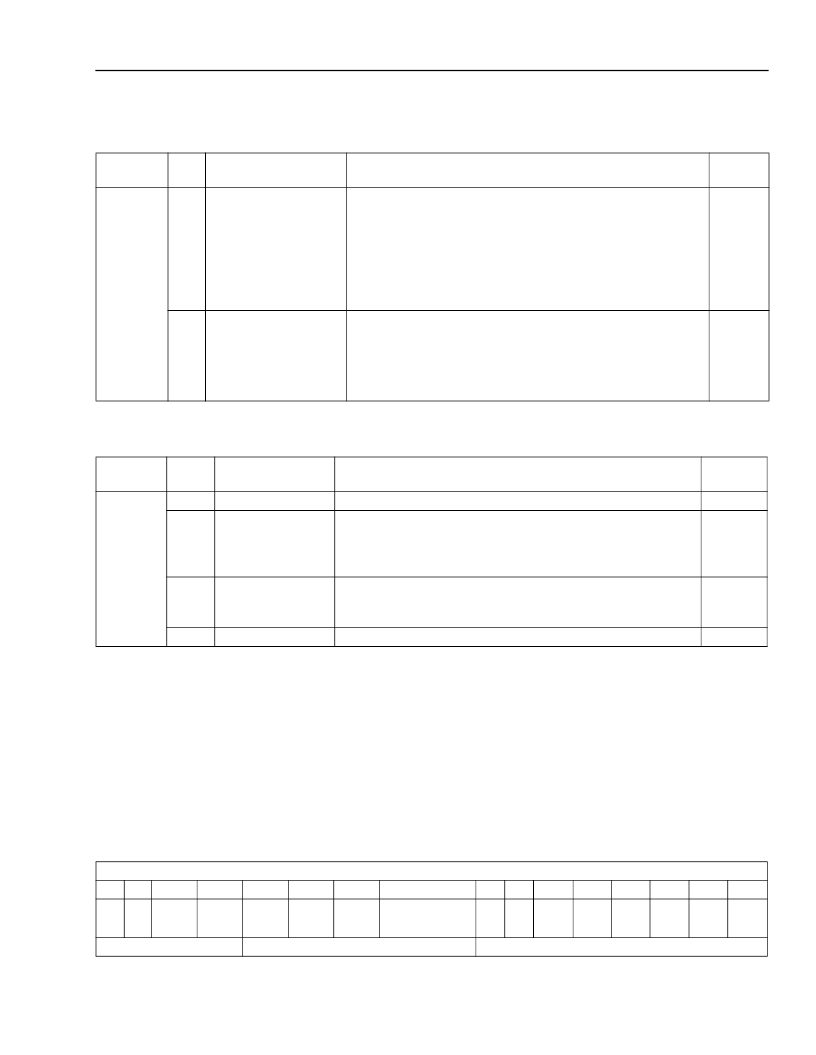
Table 378. FRM_TSLR32, Transmit Signaling Link Register 32 (R/W)
(continued)
Address
*
Bit
Name
* See
Table 376
for values of L and T.
Table 379. FRM_TSLR33, Transmit Signaling Link Register 33 (COR)
* See
Table 376
for values of L and T.
12.10 Performance Monitor Per Link Registers
The following tables describe the functions of all bits in the register map. Counters are programmable to either roll-
over or saturate, and may be programmed to clear on read.
Registers are only provisionable to clear-on-read (COR).
For each address, the register bits are identified as either read/write (R/W) or read only (RO), and the value of the
bits on reset are given.
Table 380. Performance Monitor Per Link Register Addressing Map
* L and P represent hexidecimal digits used for absolute addressing in
Table 382
through
Table 401
.
Function
Reset
Default
0
0x8LT21
2
FRM_T_FGSRC
F and G Source
. Indicates which entity will be the source for
the F and G values used in handling the ABCD bits.
0 = Host programmed.
1 = Sourced from the Rx system interface.
The F and G programming can be implied by the system
interface only when using the ASM CHI or the parallel sys-
tem interface.
FRM_T_SIGSRC[1:0]
Signaling Data Source.
Indicates which of the entities will
be the source for the ABCD bits.
00 = Signaling programmed by the host.
01 = Signaling extracted from the Rx line.
10 = Signaling received from the system interface.
1:0
00
Address
*
Bit
Name
Function
Reset
Default
0x000
0
0x8LT20
15:4
3
—
Reserved.
Must write to 0.
Time Slot 16 Multiframe Alignment Status
. A 0 indicates
that currently, time slot 16 multiframe alignment is not estab-
lished. A1 indicates that currently, time slot 16 multiframe
alignment has been established.
FRM_T_TS16AIS
Time Slot 16 AIS Detection Status
. If time slot 16 multi-
frame alignment is lost, this bit will reflect the detection of AIS
in time slot 16.
—
Reserved.
Must write to 0.
FRM_T_TS16A
2
0
1:0
00
Address Pins (ADDR15
—
ADDR0)
9
8
LNK1
LNK0
RXP = 0
TXP = 1
P*
15
0
14
0
13
12
11
10
7
1
6
0
5
4
3
2
1
0
LNK4
LNK3
LNK2
PM5
PM4 PM3 PM2 PM1
PM0
L*
—
相關(guān)PDF資料 |
PDF描述 |
|---|---|
| TMXF84622 | TMXF84622 155 Mbits/s/622 Mbits/s Interface SONET/SDH x84/x63 Ultramapper |
| TN2-L-H-3V | SLIM POLARIZED RELAY |
| TN2-L-H-48V | SLIM POLARIZED RELAY |
| TN2-L-H-4V | SLIM POLARIZED RELAY |
| TN2-L-H-5V | SLIM POLARIZED RELAY |
相關(guān)代理商/技術(shù)參數(shù) |
參數(shù)描述 |
|---|---|
| TMXF281553BAL2 | 制造商:Alcatel-Lucent 功能描述: 制造商:Lucent 功能描述: |
| TMXF281553BAL3C | 制造商:Agere 功能描述: 制造商:AGERE 功能描述: |
| TMXF281553BAL-3C-DB | 制造商:LSI Corporation 功能描述:Mapper E1 SONET/SDH 51Mbps/155Mbps 3.3V 456-Pin BGA Bag 制造商:LSI 功能描述:Mapper E1 SONET/SDH 51Mbps/155Mbps 3.3V 456-Pin BGA Bag |
| TMXF336251BL-3-DB | 制造商:LSI Corporation 功能描述:Mapper DS3/E3/DS0/E0 SONET/SDH 155Mbps/622Mbps 1.5V/3.3V 1152-Pin BGA Bag 制造商:LSI 功能描述:Mapper DS3/E3/DS0/E0 SONET/SDH 155Mbps/622Mbps 1.5V/3.3V 1152-Pin BGA Bag |
| TMXF84622 | 制造商:AGERE 制造商全稱:AGERE 功能描述:TMXF84622 155 Mbits/s/622 Mbits/s Interface SONET/SDH x84/x63 Ultramapper |
發(fā)布緊急采購,3分鐘左右您將得到回復(fù)。