- 您現(xiàn)在的位置:買賣IC網(wǎng) > PDF目錄383960 > TMX32C6411ZLZ (Texas Instruments, Inc.) FIXED POINT DIGITAL SIGNAL PROCESSOR PDF資料下載
參數(shù)資料
| 型號: | TMX32C6411ZLZ |
| 廠商: | Texas Instruments, Inc. |
| 元件分類: | 數(shù)字信號處理 |
| 英文描述: | FIXED POINT DIGITAL SIGNAL PROCESSOR |
| 中文描述: | 定點數(shù)字信號處理器 |
| 文件頁數(shù): | 78/119頁 |
| 文件大小: | 1742K |
| 代理商: | TMX32C6411ZLZ |
第1頁第2頁第3頁第4頁第5頁第6頁第7頁第8頁第9頁第10頁第11頁第12頁第13頁第14頁第15頁第16頁第17頁第18頁第19頁第20頁第21頁第22頁第23頁第24頁第25頁第26頁第27頁第28頁第29頁第30頁第31頁第32頁第33頁第34頁第35頁第36頁第37頁第38頁第39頁第40頁第41頁第42頁第43頁第44頁第45頁第46頁第47頁第48頁第49頁第50頁第51頁第52頁第53頁第54頁第55頁第56頁第57頁第58頁第59頁第60頁第61頁第62頁第63頁第64頁第65頁第66頁第67頁第68頁第69頁第70頁第71頁第72頁第73頁第74頁第75頁第76頁第77頁當(dāng)前第78頁第79頁第80頁第81頁第82頁第83頁第84頁第85頁第86頁第87頁第88頁第89頁第90頁第91頁第92頁第93頁第94頁第95頁第96頁第97頁第98頁第99頁第100頁第101頁第102頁第103頁第104頁第105頁第106頁第107頁第108頁第109頁第110頁第111頁第112頁第113頁第114頁第115頁第116頁第117頁第118頁第119頁
SPRS196H MARCH 2002 REVISED JULY 2004
78
POST OFFICE BOX 1443
HOUSTON, TEXAS 772511443
PROGRAMMABLE SYNCHRONOUS INTERFACE TIMING
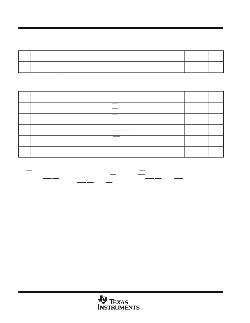
timing requirements for programmable synchronous interface cycles (see Figure 24)
NO.
300
UNIT
MIN
MAX
6
tsu(EDV-EKOxH)
th(EKOxH-EDV)
Setup time, read EDx valid before ECLKOUTx high
6.4
ns
7
Hold time, read EDx valid after ECLKOUTx high
1.5
ns
switching characteristics over recommended operating conditions for programmable
synchronous interface cycles
(see Figure 24Figure 26)
NO.
PARAMETER
300
UNIT
MIN
MAX
1
td(EKOxH-CEV)
td(EKOxH-BEV)
td(EKOxH-BEIV)
td(EKOxH-EAV)
td(EKOxH-EAIV)
td(EKOxH-ADSV)
td(EKOxH-OEV)
td(EKOxH-EDV)
td(EKOxH-EDIV)
td(EKOxH-WEV)
Delay time, ECLKOUTx high to CEx valid
1.3
9.7
ns
2
Delay time, ECLKOUTx high to BEx valid
9.7
ns
3
Delay time, ECLKOUTx high to BEx invalid
1.3
ns
4
Delay time, ECLKOUTx high to EAx valid
9.7
ns
5
Delay time, ECLKOUTx high to EAx invalid
1.3
ns
8
Delay time, ECLKOUTx high to SADS/SRE valid
1.3
9.7
ns
9
Delay time, ECLKOUTx high to, SOE valid
1.3
9.7
ns
10
Delay time, ECLKOUTx high to EDx valid
9.7
ns
11
Delay time, ECLKOUTx high to EDx invalid
1.3
ns
12
Delay time, ECLKOUTx high to SWE valid
1.3
9.7
ns
The following parameters are programmable via the EMIF CE Space Secondary Control register (CExSEC):
Read latency (SYNCRL): 0-, 1-, 2-, or 3-cycle read latency
Write latency (SYNCWL): 0-, 1-, 2-, or 3-cycle write latency
CEx assertion length (CEEXT): For standard SBSRAM or ZBT SRAM interface, CEx goes inactive after the final command has been issued
(CEEXT = 0). For synchronous FIFO interface with glue, CEx is active when SOE is active (CEEXT = 1).
Function of SADS/SRE (RENEN): For standard SBSRAM or ZBT SRAM interface, SADS/SRE acts as SADS with deselect cycles
(RENEN = 0). For FIFO interface, SADS/SRE acts as SRE with NO deselect cycles (RENEN = 1).
Synchronization clock (SNCCLK): Synchronized to ECLKOUT1 or ECLKOUT2
相關(guān)PDF資料 |
PDF描述 |
|---|---|
| TMP32C6411AGLZ | FIXED POINT DIGITAL SIGNAL PROCESSOR |
| TMP32C6411GLZ | FIXED POINT DIGITAL SIGNAL PROCESSOR |
| TMX32C6411GLZ | Anti-Static Storage Bags; External Height:5"; External Width:3"; Thickness:0.12" |
| TMP320C6411GLZ | FIXED POINT DIGITAL SIGNAL PROCESSOR |
| TMP470R1B768PGE | 16/32-Bit RISC Flash Microcontroller |
相關(guān)代理商/技術(shù)參數(shù) |
參數(shù)描述 |
|---|---|
| TMX32C6414EGLZ6E3 | 制造商:Rochester Electronics LLC 功能描述:- Bulk |
| TMX32C6415EGLZ5E0 | 制造商:Rochester Electronics LLC 功能描述:LAPLACE, REV. 2.0, 500 MHZ, 100 MHZ EMIF - Bulk |
| TMX32C6416EGLZ5E0 | 制造商:Rochester Electronics LLC 功能描述:- Bulk |
| TMX32TCI6482BZTZA2 | 制造商:Texas Instruments 功能描述: |
| TMX32TCI6616BXCYPA | 制造商:Texas Instruments 功能描述: |
發(fā)布緊急采購,3分鐘左右您將得到回復(fù)。