- 您現(xiàn)在的位置:買賣IC網(wǎng) > PDF目錄382635 > TMS320F2812PGFMEP (Texas Instruments, Inc.) Digital Signal Processors PDF資料下載
參數(shù)資料
| 型號: | TMS320F2812PGFMEP |
| 廠商: | Texas Instruments, Inc. |
| 元件分類: | 數(shù)字信號處理 |
| 英文描述: | Digital Signal Processors |
| 中文描述: | 數(shù)字信號處理器 |
| 文件頁數(shù): | 43/159頁 |
| 文件大?。?/td> | 2084K |
| 代理商: | TMS320F2812PGFMEP |
第1頁第2頁第3頁第4頁第5頁第6頁第7頁第8頁第9頁第10頁第11頁第12頁第13頁第14頁第15頁第16頁第17頁第18頁第19頁第20頁第21頁第22頁第23頁第24頁第25頁第26頁第27頁第28頁第29頁第30頁第31頁第32頁第33頁第34頁第35頁第36頁第37頁第38頁第39頁第40頁第41頁第42頁當(dāng)前第43頁第44頁第45頁第46頁第47頁第48頁第49頁第50頁第51頁第52頁第53頁第54頁第55頁第56頁第57頁第58頁第59頁第60頁第61頁第62頁第63頁第64頁第65頁第66頁第67頁第68頁第69頁第70頁第71頁第72頁第73頁第74頁第75頁第76頁第77頁第78頁第79頁第80頁第81頁第82頁第83頁第84頁第85頁第86頁第87頁第88頁第89頁第90頁第91頁第92頁第93頁第94頁第95頁第96頁第97頁第98頁第99頁第100頁第101頁第102頁第103頁第104頁第105頁第106頁第107頁第108頁第109頁第110頁第111頁第112頁第113頁第114頁第115頁第116頁第117頁第118頁第119頁第120頁第121頁第122頁第123頁第124頁第125頁第126頁第127頁第128頁第129頁第130頁第131頁第132頁第133頁第134頁第135頁第136頁第137頁第138頁第139頁第140頁第141頁第142頁第143頁第144頁第145頁第146頁第147頁第148頁第149頁第150頁第151頁第152頁第153頁第154頁第155頁第156頁第157頁第158頁第159頁
Functional Overview
43
March 2004 Revised October 2004
SGUS051A
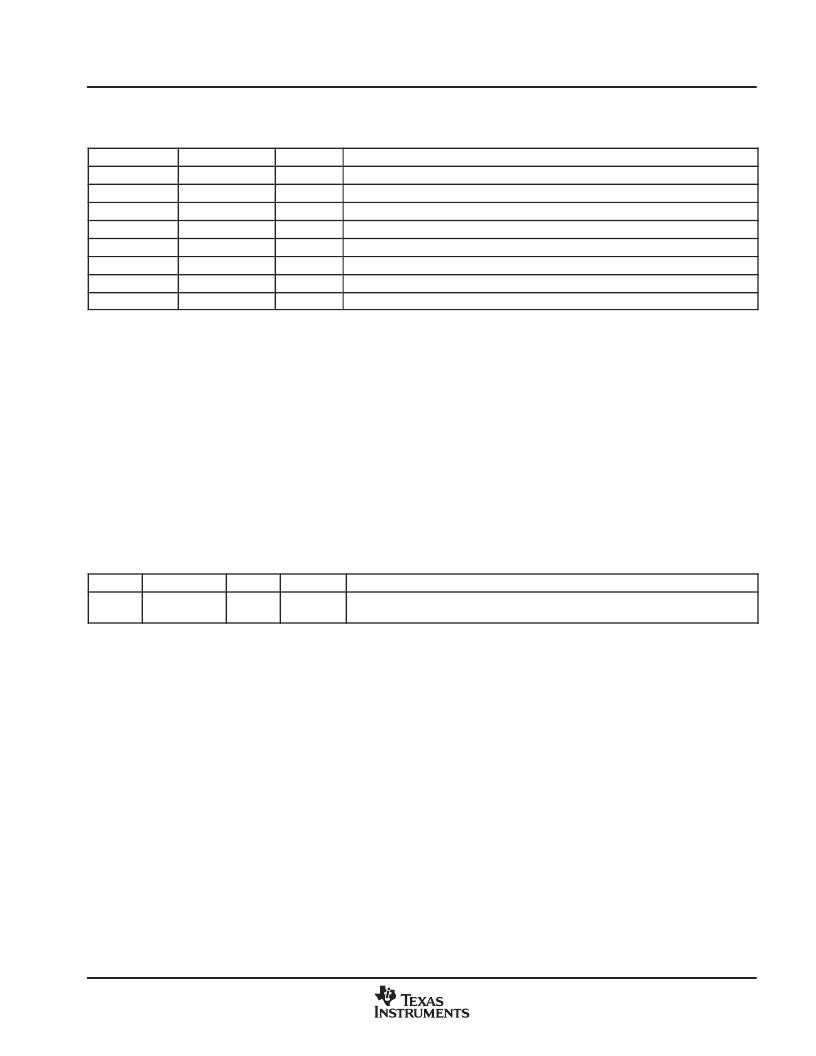
The operation and timing of the external interface, can be controlled by the registers listed in Table 38.
Table 38. XINTF Configuration and Control Register Mappings
NAME
ADDRESS
SIZE (x16)
DESCRIPTION
XTIMING0
0x00 0B20
2
XINTF Timing Register, Zone 0 can access as two 16-bit registers or one 32-bit register
XTIMING1
0x00 0B22
2
XINTF Timing Register, Zone 1 can access as two 16-bit registers or one 32-bit register
XTIMING2
0x00 0B24
2
XINTF Timing Register, Zone 2 can access as two 16-bit registers or one 32-bit register
XTIMING6
0x00 0B2C
2
XINTF Timing Register, Zone 6 can access as two 16-bit registers or one 32-bit register
XTIMING7
0x00 0B2E
2
XINTF Timing Register, Zone 7 can access as two 16-bit registers or one 32-bit register
XINTCNF2
0x00 0B34
2
XINTF Configuration Register can access as two 16-bit registers or one 32-bit register
XBANK
0x00 0B38
1
XINTF Bank Control Register
XREVISION
0x00 0B3A
1
XINTF Revision Register
3.5.1
Timing Registers
XINTF signal timing can be tuned to match specific external device requirements such as setup and hold times
to strobe signals for contention avoidance and maximizing bus efficiency. The timing parameters can be
configured individually for each zone. This allows the programmer to maximize the efficiency of the bus, based
on the type of memory or peripheral that the user needs to access. All XINTF timing values are with respect
to XTIMCLK, which is equal to or one-half of the SYSCLKOUT rate, as shown in Figure 628.
For detailed information on the XINTF timing and configuration register bit fields, see the
TMS320F28x DSP
External Interface (XINTF) Reference Guide
(literature number SPRU067).
3.5.2
XREVISION Register
The XREVISION register contains a unique number to identify the particular version of XINTF used in the
product. For the 2812, this register will be configured as described in Table 39.
Table 39. XREVISION Register Bit Definitions
BIT(S)
NAME
TYPE
RESET
DESCRIPTION
150
REVISION
R
0x0004
Current XINTF Revision. For internal use/reference. Test purposes only. Subject to
change.
相關(guān)PDF資料 |
PDF描述 |
|---|---|
| TMS320F2810PGFAEP | Digital Signal Processors |
| TMX20F2810PBKAEP | Digital Signal Processors |
| TMS320LC2404APGA | DSP CONTROLLERS |
| TMP320LC2401APAGA | DSP CONTROLLERS |
| TMP320LC2401APAGS | DSP CONTROLLERS |
相關(guān)代理商/技術(shù)參數(shù) |
參數(shù)描述 |
|---|---|
| TMS320F2812PGFQ | 功能描述:數(shù)字信號處理器和控制器 - DSP, DSC 32-Bit Digital Sig Controller w/Flash RoHS:否 制造商:Microchip Technology 核心:dsPIC 數(shù)據(jù)總線寬度:16 bit 程序存儲(chǔ)器大小:16 KB 數(shù)據(jù) RAM 大小:2 KB 最大時(shí)鐘頻率:40 MHz 可編程輸入/輸出端數(shù)量:35 定時(shí)器數(shù)量:3 設(shè)備每秒兆指令數(shù):50 MIPs 工作電源電壓:3.3 V 最大工作溫度:+ 85 C 封裝 / 箱體:TQFP-44 安裝風(fēng)格:SMD/SMT |
| TMS320F2812PGFQ | 制造商:Texas Instruments 功能描述:Digital Signal Processor |
| TMS320F2812PGFS | 功能描述:數(shù)字信號處理器和控制器 - DSP, DSC 32-Bit Digital Sig Controller w/Flash RoHS:否 制造商:Microchip Technology 核心:dsPIC 數(shù)據(jù)總線寬度:16 bit 程序存儲(chǔ)器大小:16 KB 數(shù)據(jù) RAM 大小:2 KB 最大時(shí)鐘頻率:40 MHz 可編程輸入/輸出端數(shù)量:35 定時(shí)器數(shù)量:3 設(shè)備每秒兆指令數(shù):50 MIPs 工作電源電壓:3.3 V 最大工作溫度:+ 85 C 封裝 / 箱體:TQFP-44 安裝風(fēng)格:SMD/SMT |
| TMS320F2812ZHHA | 功能描述:數(shù)字信號處理器和控制器 - DSP, DSC 32-Bit Digital Sig Controller w/Flash RoHS:否 制造商:Microchip Technology 核心:dsPIC 數(shù)據(jù)總線寬度:16 bit 程序存儲(chǔ)器大小:16 KB 數(shù)據(jù) RAM 大小:2 KB 最大時(shí)鐘頻率:40 MHz 可編程輸入/輸出端數(shù)量:35 定時(shí)器數(shù)量:3 設(shè)備每秒兆指令數(shù):50 MIPs 工作電源電壓:3.3 V 最大工作溫度:+ 85 C 封裝 / 箱體:TQFP-44 安裝風(fēng)格:SMD/SMT |
| TMS320F2812ZHHAR | 功能描述:數(shù)字信號處理器和控制器 - DSP, DSC 32B DIGITAL SIGNAL CONTROLLER RoHS:否 制造商:Microchip Technology 核心:dsPIC 數(shù)據(jù)總線寬度:16 bit 程序存儲(chǔ)器大小:16 KB 數(shù)據(jù) RAM 大小:2 KB 最大時(shí)鐘頻率:40 MHz 可編程輸入/輸出端數(shù)量:35 定時(shí)器數(shù)量:3 設(shè)備每秒兆指令數(shù):50 MIPs 工作電源電壓:3.3 V 最大工作溫度:+ 85 C 封裝 / 箱體:TQFP-44 安裝風(fēng)格:SMD/SMT |
發(fā)布緊急采購,3分鐘左右您將得到回復(fù)。