- 您現(xiàn)在的位置:買賣IC網(wǎng) > PDF目錄382635 > TMS320F2812PGFMEP (Texas Instruments, Inc.) Digital Signal Processors PDF資料下載
參數(shù)資料
| 型號: | TMS320F2812PGFMEP |
| 廠商: | Texas Instruments, Inc. |
| 元件分類: | 數(shù)字信號處理 |
| 英文描述: | Digital Signal Processors |
| 中文描述: | 數(shù)字信號處理器 |
| 文件頁數(shù): | 126/159頁 |
| 文件大小: | 2084K |
| 代理商: | TMS320F2812PGFMEP |
第1頁第2頁第3頁第4頁第5頁第6頁第7頁第8頁第9頁第10頁第11頁第12頁第13頁第14頁第15頁第16頁第17頁第18頁第19頁第20頁第21頁第22頁第23頁第24頁第25頁第26頁第27頁第28頁第29頁第30頁第31頁第32頁第33頁第34頁第35頁第36頁第37頁第38頁第39頁第40頁第41頁第42頁第43頁第44頁第45頁第46頁第47頁第48頁第49頁第50頁第51頁第52頁第53頁第54頁第55頁第56頁第57頁第58頁第59頁第60頁第61頁第62頁第63頁第64頁第65頁第66頁第67頁第68頁第69頁第70頁第71頁第72頁第73頁第74頁第75頁第76頁第77頁第78頁第79頁第80頁第81頁第82頁第83頁第84頁第85頁第86頁第87頁第88頁第89頁第90頁第91頁第92頁第93頁第94頁第95頁第96頁第97頁第98頁第99頁第100頁第101頁第102頁第103頁第104頁第105頁第106頁第107頁第108頁第109頁第110頁第111頁第112頁第113頁第114頁第115頁第116頁第117頁第118頁第119頁第120頁第121頁第122頁第123頁第124頁第125頁當(dāng)前第126頁第127頁第128頁第129頁第130頁第131頁第132頁第133頁第134頁第135頁第136頁第137頁第138頁第139頁第140頁第141頁第142頁第143頁第144頁第145頁第146頁第147頁第148頁第149頁第150頁第151頁第152頁第153頁第154頁第155頁第156頁第157頁第158頁第159頁
Electrical Specifications
125
March 2004 Revised October 2004
SGUS051A
6.25
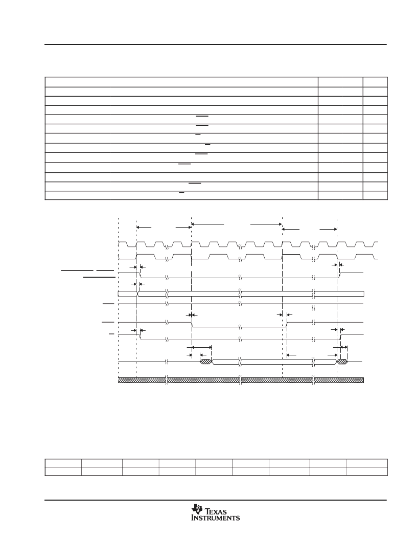
External Interface Write Timing
Table 629. External Memory Interface Write Switching Characteristics
PARAMETER
MIN
MAX
UNIT
td(XCOH-XZCSL)
td(XCOHL-XZCSH)
td(XCOH-XA)
td(XCOHL-XWEL)
td(XCOHL-XWEH)
td(XCOH-XRNWL)
td(XCOHL-XRNWH)
ten(XD)XWEL
td(XWEL-XD)
th(XA)XZCSH
th(XD)XWE
tdis(XD)XRNW
During inactive cycles, the XINTF address bus will always hold the last address put out on the bus. This includes alignment cycles.
TW = Trail period, write access. See Table 625.
Delay time, XCLKOUT high to zone chip-select active low
1
ns
Delay time, XCLKOUT high or low to zone chip-select inactive high
2
3
ns
Delay time, XCLKOUT high to address valid
2
ns
Delay time, XCLKOUT high/low to XWE low
2
ns
Delay time, XCLKOUT high/low to XWE high
2
ns
Delay time, XCLKOUT high to XR/W low
1
ns
Delay time, XCLKOUT high/low to XR/W high
2
1
ns
Enable time, data bus driven from XWE low
0
ns
Delay time, data valid after XWE active low
4
ns
Hold time, address valid after zone chip-select inactive high
ns
Hold time, write data valid after XWE inactive high
TW2
ns
Data bus disabled after XR/W inactive high
4
ns
Lead
Active
Trail
td(XCOH-XZCSL)
td(XCOH-XA)
td(XCOHL-XWEL)
td(XCOHL-XWEH)
td(XCOHL-XZCSH)
ten(XD)XWEL
th(XD)XWEH
tdis(XD)XRNW
XCLKOUT=XTIMCLK
XCLKOUT=1/2 XTIMCLK
XZCS0AND1, XZCS2,
XZCS6AND7
XA[0:18]
XRD
XWE
XR/W
XD[0:15]
NOTES: A. All XINTF accesses (lead period) begin on the rising edge of XCLKOUT. When necessary, the device will insert an alignment
cycle before an access to meet this requirement.
B. During alignment cycles, all signals will transition to their inactive state.
C. For USEREADY = 0, the external XREADY input signal is ignored.
D. XA[0:18] will hold the last address put on the bus during inactive cycles, including alignment cycles.
td(XCOH-XRNWL)
td(XCOHL-XRNWH)
DOUT
XREADY
td(XWEL-XD)
Figure 630. Example Write Access
XTIMING register parameters used for this example:
XRDLEAD
N/A
N/A = “Don’t care” for this example
XRDACTIVE
N/A
XRDTRAIL
N/A
USEREADY
X2TIMING
XWRLEAD
XWRACTIVE
XWRTRAIL
READYMODE
N/A
0
0
≥
1
≥
0
≥
0
相關(guān)PDF資料 |
PDF描述 |
|---|---|
| TMS320F2810PGFAEP | Digital Signal Processors |
| TMX20F2810PBKAEP | Digital Signal Processors |
| TMS320LC2404APGA | DSP CONTROLLERS |
| TMP320LC2401APAGA | DSP CONTROLLERS |
| TMP320LC2401APAGS | DSP CONTROLLERS |
相關(guān)代理商/技術(shù)參數(shù) |
參數(shù)描述 |
|---|---|
| TMS320F2812PGFQ | 功能描述:數(shù)字信號處理器和控制器 - DSP, DSC 32-Bit Digital Sig Controller w/Flash RoHS:否 制造商:Microchip Technology 核心:dsPIC 數(shù)據(jù)總線寬度:16 bit 程序存儲器大小:16 KB 數(shù)據(jù) RAM 大小:2 KB 最大時鐘頻率:40 MHz 可編程輸入/輸出端數(shù)量:35 定時器數(shù)量:3 設(shè)備每秒兆指令數(shù):50 MIPs 工作電源電壓:3.3 V 最大工作溫度:+ 85 C 封裝 / 箱體:TQFP-44 安裝風(fēng)格:SMD/SMT |
| TMS320F2812PGFQ | 制造商:Texas Instruments 功能描述:Digital Signal Processor |
| TMS320F2812PGFS | 功能描述:數(shù)字信號處理器和控制器 - DSP, DSC 32-Bit Digital Sig Controller w/Flash RoHS:否 制造商:Microchip Technology 核心:dsPIC 數(shù)據(jù)總線寬度:16 bit 程序存儲器大小:16 KB 數(shù)據(jù) RAM 大小:2 KB 最大時鐘頻率:40 MHz 可編程輸入/輸出端數(shù)量:35 定時器數(shù)量:3 設(shè)備每秒兆指令數(shù):50 MIPs 工作電源電壓:3.3 V 最大工作溫度:+ 85 C 封裝 / 箱體:TQFP-44 安裝風(fēng)格:SMD/SMT |
| TMS320F2812ZHHA | 功能描述:數(shù)字信號處理器和控制器 - DSP, DSC 32-Bit Digital Sig Controller w/Flash RoHS:否 制造商:Microchip Technology 核心:dsPIC 數(shù)據(jù)總線寬度:16 bit 程序存儲器大小:16 KB 數(shù)據(jù) RAM 大小:2 KB 最大時鐘頻率:40 MHz 可編程輸入/輸出端數(shù)量:35 定時器數(shù)量:3 設(shè)備每秒兆指令數(shù):50 MIPs 工作電源電壓:3.3 V 最大工作溫度:+ 85 C 封裝 / 箱體:TQFP-44 安裝風(fēng)格:SMD/SMT |
| TMS320F2812ZHHAR | 功能描述:數(shù)字信號處理器和控制器 - DSP, DSC 32B DIGITAL SIGNAL CONTROLLER RoHS:否 制造商:Microchip Technology 核心:dsPIC 數(shù)據(jù)總線寬度:16 bit 程序存儲器大小:16 KB 數(shù)據(jù) RAM 大小:2 KB 最大時鐘頻率:40 MHz 可編程輸入/輸出端數(shù)量:35 定時器數(shù)量:3 設(shè)備每秒兆指令數(shù):50 MIPs 工作電源電壓:3.3 V 最大工作溫度:+ 85 C 封裝 / 箱體:TQFP-44 安裝風(fēng)格:SMD/SMT |
發(fā)布緊急采購,3分鐘左右您將得到回復(fù)。