- 您現(xiàn)在的位置:買賣IC網(wǎng) > PDF目錄384004 > TLC320AD75C (Texas Instruments, Inc.) 20-Bit Sigma-Delta Stereo ADA Circuit PDF資料下載
參數(shù)資料
| 型號: | TLC320AD75C |
| 廠商: | Texas Instruments, Inc. |
| 英文描述: | 20-Bit Sigma-Delta Stereo ADA Circuit |
| 中文描述: | 20位Σ-Δ立體聲電路反傾銷協(xié)定 |
| 文件頁數(shù): | 17/43頁 |
| 文件大小: | 211K |
| 代理商: | TLC320AD75C |
第1頁第2頁第3頁第4頁第5頁第6頁第7頁第8頁第9頁第10頁第11頁第12頁第13頁第14頁第15頁第16頁當(dāng)前第17頁第18頁第19頁第20頁第21頁第22頁第23頁第24頁第25頁第26頁第27頁第28頁第29頁第30頁第31頁第32頁第33頁第34頁第35頁第36頁第37頁第38頁第39頁第40頁第41頁第42頁第43頁
2–5
2.7
TEST1 and TEST2 are reserved for factory test and are tied to digital ground (V
SS1
).
2.8
Master Mode for ADC
Configured as the master device (M_S is connected to V
DD1
), the TLC320AD75C generates LRCKA and
SCLKA from MCLKI. These signals are provided for synchronizing the serial port of a digital signal processor
(DSP) or other control devices.
Test
LRCKA is generated internally from MCLKI. The frequency of LRCKA is fixed at the sampling frequency,
f
s
(MCLKI/256). During the high period of LRCKA, the left channel data is serially shifted to the output; during
the low period, the right channel data is shifted to the output (ADOUT). The conversion cycle is synchronized
with the rising edge of LRCKA.
Figure 2–4 (master mode) shows 20-bit data, MSB first, ADOUT data shifted out of the TLC320AD75 during
the first 20 SCLKA periods of the 32 SCLKA periods for both left and right channel data.
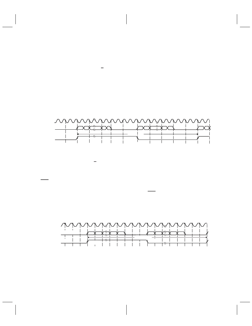
20-BIT MASTER MODE
SCLKA
MSB
LSB
19
18
. . .
1
0
19
18
. . .
1
0
19
64 SCLKs
ADOUT
LRCKA
Right
Left
18
Output
Output
Output
MSB
LSB
MSB
Figure 2–4. ADC Audio-Data Serial Timing – Master Mode
2.9
Configured as a slave device (M_S is connected to V
SS1
), the TLC320AD75C receives LRCKA and SCLKA
as inputs. The conversion cycle is synchronized to the rising edge of LRCKA, and the data is synchronized
to the falling edge of SCLKA. SCLKA must meet the setup requirements specified in the recommended
operating conditions section. Synchronization of the slave mode is accomplished with the rising edge of
DPD.
Slave Mode for ADC
The slave mode is shown in Figure 2–5. SCLKA and LRCKA are externally generated and sourced. The
first rising edges of SCLKA and LRCKA after the rising edge of DPD initiate the conversion cycle (see
Section 2.8, Master Mode for ADCfor signal functions).
Figure 2–5 (slave mode) shows 20-bit data, MSB first, and ADOUT data shifted out of the TLC320AD75
during the first 20 SCLKA periods of the 32 SCLKA periods for both left and right channel data.
19
18
. . .
1
0
19
18
. . .
1
0
64 SCLKs
ADOUT
LRCKA
20-BIT SLAVE MODE
output
input
Left
Right
SCLKA
input
MSB
LSB
MSB
LSB
Figure 2–5. ADC Audio-Data Serial Timing – Slave Mode
2.10 Digital-Audio Data Interface for DAC
The conversion cycle is synchronized to the rising edge of LRCKD, and the data must meet the setup
requirements specified in the timing requirements table. The input data is 16 or 20 bits with the MSB or LSB
first as selected in the system register. The recommended SCLKD frequency is 64
×
f
s
. Figure 2–6
illustrates the input timing.
相關(guān)PDF資料 |
PDF描述 |
|---|---|
| TLC320AD77C | 24-BIT 96 kHz STEREO AUDIO CODEC |
| TLC320AD80C | Audio Processor Subsystem |
| TLC320AD81CDBT | Stereo Audio Digital Equalizer DC |
| TLC320AD81C | Stereo Audio Digital Equalizer DC |
| TLC339CDB | LinCMOSE MICROPOWER QUAD COMPARATORS |
相關(guān)代理商/技術(shù)參數(shù) |
參數(shù)描述 |
|---|---|
| TLC320AD75CDL | 制造商:Texas Instruments 功能描述: |
| TLC320AD77 | 制造商:TI 制造商全稱:Texas Instruments 功能描述:24-Bit 96 kHz Stereo Audio Codec |
| TLC320AD77C | 制造商:TI 制造商全稱:Texas Instruments 功能描述:24-BIT 96 kHz STEREO AUDIO CODEC |
| TLC320AD77CDB | 功能描述:接口—CODEC STEREO AUDIO ADA RoHS:否 制造商:Texas Instruments 類型: 分辨率: 轉(zhuǎn)換速率:48 kSPs 接口類型:I2C ADC 數(shù)量:2 DAC 數(shù)量:4 工作電源電壓:1.8 V, 2.1 V, 2.3 V to 5.5 V 最大工作溫度:+ 85 C 安裝風(fēng)格:SMD/SMT 封裝 / 箱體:DSBGA-81 封裝:Reel |
| TLC320AD77CDBG4 | 功能描述:接口—CODEC STEREO AUDIO ADA RoHS:否 制造商:Texas Instruments 類型: 分辨率: 轉(zhuǎn)換速率:48 kSPs 接口類型:I2C ADC 數(shù)量:2 DAC 數(shù)量:4 工作電源電壓:1.8 V, 2.1 V, 2.3 V to 5.5 V 最大工作溫度:+ 85 C 安裝風(fēng)格:SMD/SMT 封裝 / 箱體:DSBGA-81 封裝:Reel |
發(fā)布緊急采購,3分鐘左右您將得到回復(fù)。