- 您現(xiàn)在的位置:買(mǎi)賣(mài)IC網(wǎng) > PDF目錄383953 > TLC2942PW (Texas Instruments, Inc.) HIGH-PERFORMANCE DUAL PHASE-LOCKED LOOP BUILDING BLOCK PDF資料下載
參數(shù)資料
| 型號(hào): | TLC2942PW |
| 廠商: | Texas Instruments, Inc. |
| 英文描述: | HIGH-PERFORMANCE DUAL PHASE-LOCKED LOOP BUILDING BLOCK |
| 中文描述: | 高效能雙鎖相環(huán)積木 |
| 文件頁(yè)數(shù): | 18/28頁(yè) |
| 文件大?。?/td> | 459K |
| 代理商: | TLC2942PW |
第1頁(yè)第2頁(yè)第3頁(yè)第4頁(yè)第5頁(yè)第6頁(yè)第7頁(yè)第8頁(yè)第9頁(yè)第10頁(yè)第11頁(yè)第12頁(yè)第13頁(yè)第14頁(yè)第15頁(yè)第16頁(yè)第17頁(yè)當(dāng)前第18頁(yè)第19頁(yè)第20頁(yè)第21頁(yè)第22頁(yè)第23頁(yè)第24頁(yè)第25頁(yè)第26頁(yè)第27頁(yè)第28頁(yè)
TLC2942
HIGH-PERFORMANCE DUAL PHASE-LOCKED LOOP BUILDING BLOCK
SLAS146B – NOVEMBER 1996 – REVISED JUNE 1997
18
POST OFFICE BOX 655303
DALLAS, TEXAS 75265
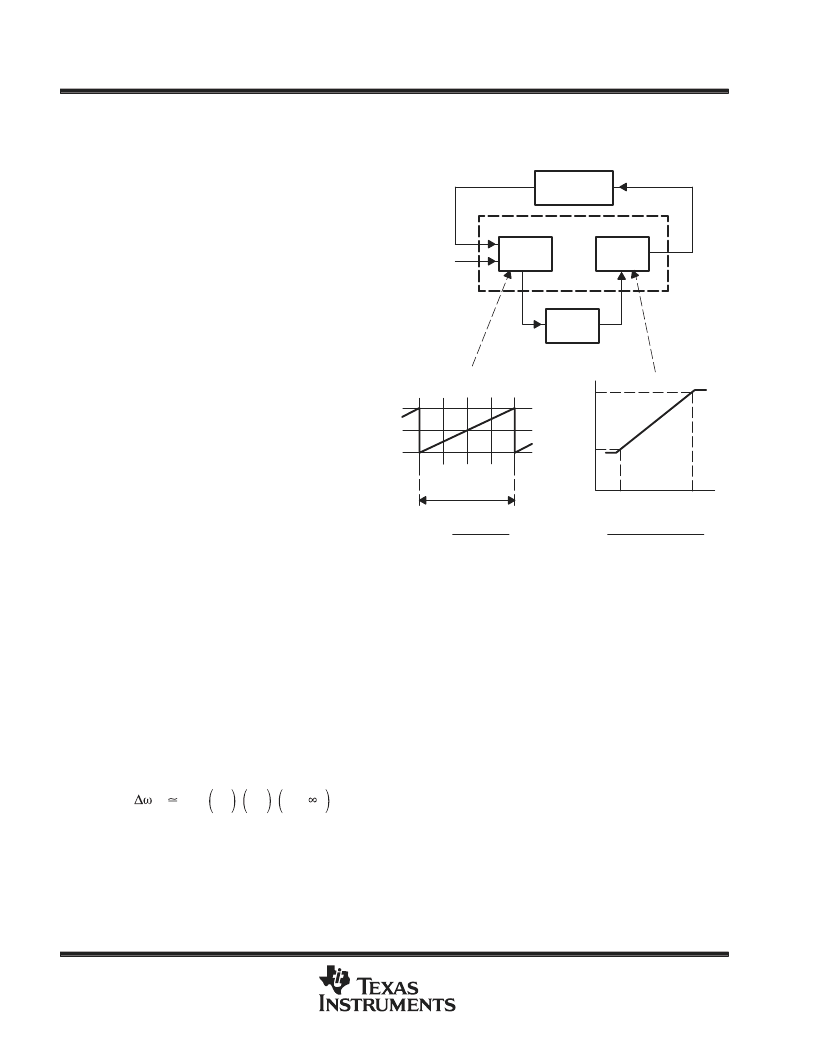
APPLICATION INFORMATION
gain of VCO and PFD
Figure 24 is a block diagram of the PLL. The
divider N value depends on the input frequency
and the desired VCO output frequency according
to the system application requirements. The K
p
and K
V
values are obtained from the operating
characteristics of the device as shown in Figure
24. K
p
is defined from the phase detector V
OL
and
V
OH
specifications and the equation shown in
Figure 24(b). K
V
is defined from Figures 8, 9, 10,
and 11 as shown in Figure 24(c).
The parameters for the block diagram with the
units are as follows:
K
V
: VCO gain (rad/s/V)
K
p
: PFD gain (V/rad)
K
f
: LPF gain (V/V)
K
N
: countdown divider gain (1/N)
external counter
When a large N counter is required by the
application, there is a possibility that the PLL
response becomes slow due to the counter
response delay time. In the case of a high
frequency application, the counter delay time
should be accounted for in the overall PLL design.
R
BIAS
The external bias resistor sets the VCO center frequency with 1/2 V
DD
applied to the VCOIN terminal. However,
for optimum temperature performance, a resistor value of 3.3 k
with a 3-V supply, or a resistor value of
2.5 k
for a 5-V supply is recommended. For the most accurate results, a metal-film resistor is the better choice,
but a carbon-compositiion resistor can be used with excellent results also. A 0.22-
μ
F capacitor should be
connected from the BIAS terminal to ground as close to the device terminals as possible.
hold-in range
From the technical literature, the maximum hold-in range for an input frequency step for the three types of filter
configurations shown in Figure 25 is as follows:
H
0.8 Kp
KV
Kf(
)
Where
K
f
(
∞
) = the filter transfer function value at
ω
=
∞
(1)
Divider
(KN = 1/N)
PFD
(Kp)
VCO
(KV)
LPF
(Kf)
TLC2942
fREF
VOH
fMAX
fMIN
VIN MIN
VIN MAX
–2
π
2
π
–
π
0
π
Range of
Comparison
VOH
VOL
Kp =
VOH – VOL
4
π
KV =
2
π
(fMAX – fMIN)
VIN MAX – VIN MIN
(c)
Figure 24. Example of a PLL Block Diagram
(a)
(b)
相關(guān)PDF資料 |
PDF描述 |
|---|---|
| TLC32040C | ANALOG INTERFACE CIRCUITS |
| TLC32040I | ANALOG INTERFACE CIRCUITS |
| TLC32041C | ANALOG INTERFACE CIRCUITS |
| TLC32041CFN | ANALOG INTERFACE CIRCUITS |
| TLC32041I | ANALOG INTERFACE CIRCUITS |
相關(guān)代理商/技術(shù)參數(shù) |
參數(shù)描述 |
|---|---|
| TLC2943IDB | 制造商:Rochester Electronics LLC 功能描述:- Bulk |
| TLC-2C-0164 | 制造商:KATO/COILTHREAD 功能描述: |
| TLC-2C-0164W | 制造商:KATO/COILTHREAD 功能描述: |
| TLC-2C-0164Y | 制造商:KATO/COILTHREAD 功能描述: |
| TLC-2C-0246 | 制造商:KATO/COILTHREAD 功能描述: |
發(fā)布緊急采購(gòu),3分鐘左右您將得到回復(fù)。