- 您現(xiàn)在的位置:買賣IC網 > PDF目錄98109 > SN74BCT8373ADWR (TEXAS INSTRUMENTS INC) BCT/FBT SERIES, 8-BIT BOUNDARY SCAN DRIVER, TRUE OUTPUT, PDSO24 PDF資料下載
參數(shù)資料
| 型號: | SN74BCT8373ADWR |
| 廠商: | TEXAS INSTRUMENTS INC |
| 元件分類: | 總線收發(fā)器 |
| 英文描述: | BCT/FBT SERIES, 8-BIT BOUNDARY SCAN DRIVER, TRUE OUTPUT, PDSO24 |
| 封裝: | PLASTIC, SO-24 |
| 文件頁數(shù): | 8/26頁 |
| 文件大小: | 487K |
| 代理商: | SN74BCT8373ADWR |
SN54BCT8373A, SN74BCT8373A
SCAN TEST DEVICES
WITH OCTAL D-TYPE LATCHES
SCBS044F – JUNE 1990 – REVISED JULY 1996
16
POST OFFICE BOX 655303
DALLAS, TEXAS 75265
absolute maximum ratings over operating free-air temperature range (unless otherwise noted)
Supply voltage range, VCC
– 0.5 V to 7 V
. . . . . . . . . . . . . . . . . . . . . . . . . . . . . . . . . . . . . . . . . . . . . . . . . . . . . . . . . .
Input voltage range, VI: Except TMS (see Note 1)
– 0.5 V to 7 V
. . . . . . . . . . . . . . . . . . . . . . . . . . . . . . . . . . . . . .
TMS (see Note 1)
– 0.5 V to 12 V
. . . . . . . . . . . . . . . . . . . . . . . . . . . . . . . . . . . . . . . . . . .
Voltage range applied to any output in the disabled or power-off state
– 0.5 V to 5.5 V
. . . . . . . . . . . . . . . . . . . .
Voltage range applied to any output in the high state
– 0.5 V to VCC
. . . . . . . . . . . . . . . . . . . . . . . . . . . . . . . . . .
Input clamp current
– 30 mA
. . . . . . . . . . . . . . . . . . . . . . . . . . . . . . . . . . . . . . . . . . . . . . . . . . . . . . . . . . . . . . . . . . . . .
Current into any output in the low state: SN54BCT8373A (TDO)
40 mA
. . . . . . . . . . . . . . . . . . . . . . . . . . . . . . .
SN54BCT8373A (Any Q)
96 mA
. . . . . . . . . . . . . . . . . . . . . . . . . . . . .
SN74BCT8373A (TDO)
48 mA
. . . . . . . . . . . . . . . . . . . . . . . . . . . . . . .
SN74BCT8373A (Any Q)
128 mA
. . . . . . . . . . . . . . . . . . . . . . . . . . . .
Maximum power dissipation at TA = 55°C (in still air) (see Note 2): DW package
1.7 W
. . . . . . . . . . . . . . . . . .
NT package
1.3 W
. . . . . . . . . . . . . . . . . . .
Storage temperature range, Tstg
–65
°C to 150°C
. . . . . . . . . . . . . . . . . . . . . . . . . . . . . . . . . . . . . . . . . . . . . . . . . . .
Stresses beyond those listed under “absolute maximum ratings” may cause permanent damage to the device. These are stress ratings only and
functional operation of the device at these or any other conditions beyond those indicated under “recommended operating conditions” is not
implied. Exposure to absolute-maximum-rated conditions for extended periods may affect device reliability.
NOTES:
1. The input voltage rating may be exceeded if the input clamp-current rating is observed.
2. The maximum package power dissipation is calculated using a junction temperature of 150
°C and a board trace length of 750 mils,
except for the NT package, which has a trace length of zero. For more information, refer to the
Package Thermal Considerations
application note in the
ABT Advanced BiCMOS Technology Data Book, literature number SCBD002.
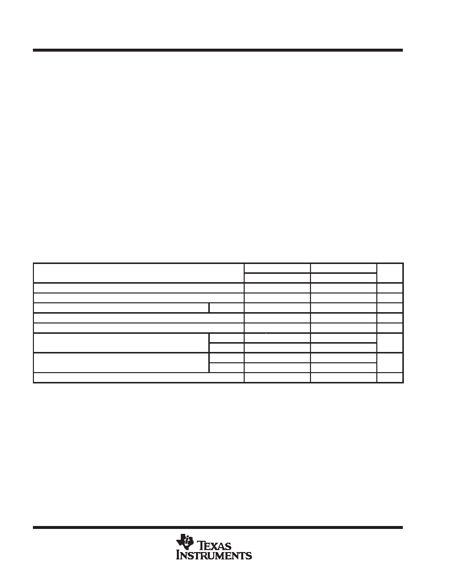
recommended operating conditions
SN54BCT8373A
SN74BCT8373A
UNIT
MIN
NOM
MAX
MIN
NOM
MAX
UNIT
VCC
Supply voltage
4.5
5
5.5
4.5
5
5.5
V
VIH
High-level input voltage
2
V
VIHH
Double-high-level input voltage
TMS
10
12
10
12
V
VIL
Low-level input voltage
0.8
V
IIK
Input clamp current
–18
mA
IOH
High level output current
TDO
–3
mA
IOH
High-level output current
Any Q
–12
–15
mA
IOL
Low level output current
TDO
20
24
mA
IOL
Low-level output current
Any Q
48
64
mA
TA
Operating free-air temperature
–55
125
0
70
°C
相關PDF資料 |
PDF描述 |
|---|---|
| SN74BCT8373NT | BCT/FBT SERIES, 8-BIT BOUNDARY SCAN DRIVER, TRUE OUTPUT, PDIP24 |
| SN74BCT8374ADWRG4 | BCT/FBT SERIES, 8-BIT BOUNDARY SCAN DRIVER, TRUE OUTPUT, PDSO24 |
| SN74BCT8374ANT | BCT/FBT SERIES, 8-BIT BOUNDARY SCAN DRIVER, TRUE OUTPUT, PDIP24 |
| SN74CB3Q16210DGVR | CB3Q/3VH/3C/2B SERIES, DUAL 10-BIT DRIVER, TRUE OUTPUT, PDSO48 |
| SN74CB3Q16811DLR | CB3Q/3VH/3C/2B SERIES, DUAL 12-BIT DRIVER, TRUE OUTPUT, PDSO56 |
相關代理商/技術參數(shù) |
參數(shù)描述 |
|---|---|
| SN74BCT8373ADWRE4 | 功能描述:特定功能邏輯 Fixed LDO Volt Reg RoHS:否 制造商:Texas Instruments 產品: 系列:SN74ABTH18502A 工作電源電壓:5 V 封裝 / 箱體:LQFP-64 封裝:Tube |
| SN74BCT8373ADWRG4 | 功能描述:特定功能邏輯 IEEE Std 1149.1 Bndry Scan Tst Devic RoHS:否 制造商:Texas Instruments 產品: 系列:SN74ABTH18502A 工作電源電壓:5 V 封裝 / 箱體:LQFP-64 封裝:Tube |
| SN74BCT8373ANT | 功能描述:特定功能邏輯 Device w/Octal D-Type Latches RoHS:否 制造商:Texas Instruments 產品: 系列:SN74ABTH18502A 工作電源電壓:5 V 封裝 / 箱體:LQFP-64 封裝:Tube |
| SN74BCT8373ANTE4 | 功能描述:特定功能邏輯 Device w/Octal D-Type Latches RoHS:否 制造商:Texas Instruments 產品: 系列:SN74ABTH18502A 工作電源電壓:5 V 封裝 / 箱體:LQFP-64 封裝:Tube |
| SN74BCT8373DW | 制造商:Rochester Electronics LLC 功能描述:- Bulk |
發(fā)布緊急采購,3分鐘左右您將得到回復。