- 您現(xiàn)在的位置:買賣IC網(wǎng) > PDF目錄98069 > S1C88832F0A0100 MICROCONTROLLER, PQFP128 PDF資料下載
參數(shù)資料
| 型號(hào): | S1C88832F0A0100 |
| 元件分類: | 微控制器/微處理器 |
| 英文描述: | MICROCONTROLLER, PQFP128 |
| 封裝: | PLASTIC, QFP-128 |
| 文件頁(yè)數(shù): | 114/160頁(yè) |
| 文件大小: | 1244K |
| 代理商: | S1C88832F0A0100 |
第1頁(yè)第2頁(yè)第3頁(yè)第4頁(yè)第5頁(yè)第6頁(yè)第7頁(yè)第8頁(yè)第9頁(yè)第10頁(yè)第11頁(yè)第12頁(yè)第13頁(yè)第14頁(yè)第15頁(yè)第16頁(yè)第17頁(yè)第18頁(yè)第19頁(yè)第20頁(yè)第21頁(yè)第22頁(yè)第23頁(yè)第24頁(yè)第25頁(yè)第26頁(yè)第27頁(yè)第28頁(yè)第29頁(yè)第30頁(yè)第31頁(yè)第32頁(yè)第33頁(yè)第34頁(yè)第35頁(yè)第36頁(yè)第37頁(yè)第38頁(yè)第39頁(yè)第40頁(yè)第41頁(yè)第42頁(yè)第43頁(yè)第44頁(yè)第45頁(yè)第46頁(yè)第47頁(yè)第48頁(yè)第49頁(yè)第50頁(yè)第51頁(yè)第52頁(yè)第53頁(yè)第54頁(yè)第55頁(yè)第56頁(yè)第57頁(yè)第58頁(yè)第59頁(yè)第60頁(yè)第61頁(yè)第62頁(yè)第63頁(yè)第64頁(yè)第65頁(yè)第66頁(yè)第67頁(yè)第68頁(yè)第69頁(yè)第70頁(yè)第71頁(yè)第72頁(yè)第73頁(yè)第74頁(yè)第75頁(yè)第76頁(yè)第77頁(yè)第78頁(yè)第79頁(yè)第80頁(yè)第81頁(yè)第82頁(yè)第83頁(yè)第84頁(yè)第85頁(yè)第86頁(yè)第87頁(yè)第88頁(yè)第89頁(yè)第90頁(yè)第91頁(yè)第92頁(yè)第93頁(yè)第94頁(yè)第95頁(yè)第96頁(yè)第97頁(yè)第98頁(yè)第99頁(yè)第100頁(yè)第101頁(yè)第102頁(yè)第103頁(yè)第104頁(yè)第105頁(yè)第106頁(yè)第107頁(yè)第108頁(yè)第109頁(yè)第110頁(yè)第111頁(yè)第112頁(yè)第113頁(yè)當(dāng)前第114頁(yè)第115頁(yè)第116頁(yè)第117頁(yè)第118頁(yè)第119頁(yè)第120頁(yè)第121頁(yè)第122頁(yè)第123頁(yè)第124頁(yè)第125頁(yè)第126頁(yè)第127頁(yè)第128頁(yè)第129頁(yè)第130頁(yè)第131頁(yè)第132頁(yè)第133頁(yè)第134頁(yè)第135頁(yè)第136頁(yè)第137頁(yè)第138頁(yè)第139頁(yè)第140頁(yè)第141頁(yè)第142頁(yè)第143頁(yè)第144頁(yè)第145頁(yè)第146頁(yè)第147頁(yè)第148頁(yè)第149頁(yè)第150頁(yè)第151頁(yè)第152頁(yè)第153頁(yè)第154頁(yè)第155頁(yè)第156頁(yè)第157頁(yè)第158頁(yè)第159頁(yè)第160頁(yè)
S1C88832/88862 TECHNICAL MANUAL
EPSON
49
5 PERIPHERAL CIRCUITS AND THEIR OPERATION (Serial Interface)
5.7.2 Mask option
Since serial interface input/output terminals are
shared with the I/O ports, serial interface terminal
specifications have necessarily been selected with
the mask option for I/O ports.
I/O port pull-up resistors
P10 (SIN) ........ s
s With resistor s
s Gate direct
P12 (SCLK) .... s
s With resistor s
s Gate direct
Each I/O port terminal is equipped with a pull-up
resistor which goes ON in input mode. A selection
can be made for each port (one bit unit) as to
whether or not the resistor will be used.
Specifications (whether the pull-up will be used or
not) of P10 (SIN) and P12 (SCLK) which will become
input terminals when using the serial interface are
decided by settings the options for the I/O port.
When "Gate direct" is selected in the serial I/F
mode, be sure that the input terminals do not go
into a floating state.
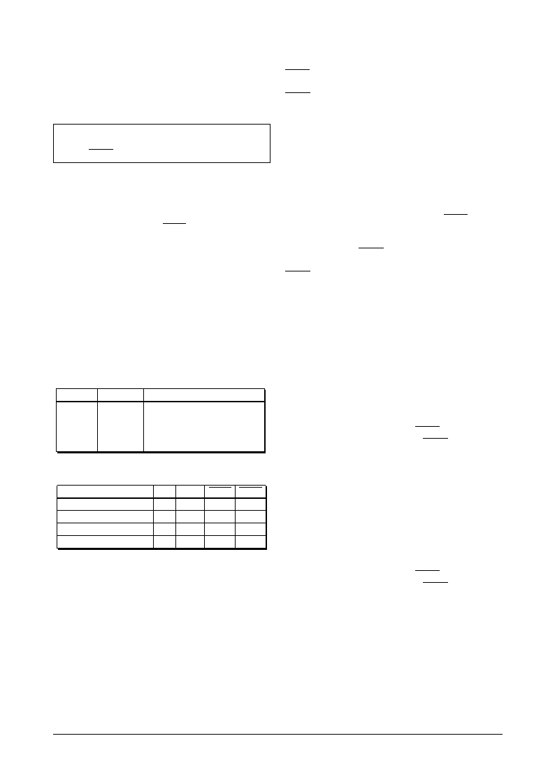
5.7.3 Transfer modes
There are four transfer modes for the serial inter-
face and mode selection is made by setting the two
bits of the mode selection registers SMD0 and
SMD1 as shown in the table below.
Table 5.7.3.1 Transfer modes
At initial reset, transfer mode is set to clock syn-
chronous master mode.
s Clock synchronous master mode
In this mode, the internal clock is utilized as a
synchronous clock for the built-in shift registers,
and clock synchronous 8-bit serial transfers can be
performed with this serial interface as the master.
Table 5.7.3.2 Terminal settings corresponding
to each transfer mode
The synchronous clock is also output from the
SCLK terminal which enables control of the
external (slave side) serial I/O device. Since the
SRDY terminal is not utilized in this mode, it can be
used as an I/O port.
Figure 5.7.3.1(a) shows the connection example of
input/output terminals in the clock synchronous
master mode.
s Clock synchronous slave mode
In this mode, a synchronous clock from the external
(master side) serial input/output device is utilized
and clock synchronous 8-bit serial transfers can be
performed with this serial interface as the slave.
The synchronous clock is input to the SCLK
terminal and is utilized by this interface as the
synchronous clock.
Furthermore, the SRDY signal indicating the
transmit-receive ready status is output from the
SRDY terminal in accordance with the serial
interface operating status.
In the slave mode, the settings for registers SCS0
and SCS1 used to select the clock source are invalid.
Figure 5.7.3.1(b) shows the connection example of
input/output terminals in the clock synchronous
slave mode.
s Asynchronous 7-bit mode
In this mode, asynchronous 7-bit transfer can be
performed. Parity check during data reception and
addition of parity bit (odd/even/none) during
transmitting can be specified and data processed in
7 bits with or without parity. Since this mode
employs the internal clock, the SCLK terminal is
not used. Furthermore, since the SRDY terminal is
not utilized either, both of these terminals can be
used as I/O ports.
Figure 5.7.3.1(c) shows the connection example of
input/output terminals in the asynchronous mode.
s Asynchronous 8-bit mode
In this mode, asynchronous 8-bit transfer can be
performed. Parity check during data reception and
addition of parity bit (odd/even/none) during
transmitting can be specified and data processed in
8 bits with or without parity. Since this mode
employs the internal clock, the SCLK terminal is
not used. Furthermore, since the SRDY terminal is
not utilized either, both of these terminals can be
used as I/O ports.
Figure 5.7.3.1(c) shows the connection example of
input/output terminals in the asynchronous mode.
SMD1
SMD0
Mode
1
0
1
0
1
0
Asynchronous 8-bit
Asynchronous 7-bit
Clock synchronous slave
Clock synchronous master
Mode
SIN
Asynchronous 8-bit
Asynchronous 7-bit
Clock synchronous slave
Clock synchronous master
P13
Output
P13
SOUT SCLK
SRDY
P12
Input
Output
Input
相關(guān)PDF資料 |
PDF描述 |
|---|---|
| S1C88848D0A0100 | 8-BIT, MROM, 8.2 MHz, MICROCONTROLLER, UUC192 |
| S1C8F360F | 8-BIT, FLASH, 8.2 MHz, MICROCONTROLLER, PQFP176 |
| S1D13305F00B | 640 X 256 PIXELS CRT CHAR OR GRPH DSPL CTLR, PQFP60 |
| S1D13305F00A | 640 X 256 PIXELS CRT CHAR OR GRPH DSPL CTLR, PQFP60 |
| S1D13600F00A | CRT OR FLAT PNL GRPH DSPL CTLR, PQFP64 |
相關(guān)代理商/技術(shù)參數(shù) |
參數(shù)描述 |
|---|---|
| S1C88848 | 制造商:EPSON 制造商全稱:EPSON 功能描述:8-bit Single Chip Microcomputer |
| S1C8F360D411000 | 功能描述:16位微控制器 - MCU 8-bit Flash 60KB LCD Dr. 51 x 32 RoHS:否 制造商:Texas Instruments 核心:RISC 處理器系列:MSP430FR572x 數(shù)據(jù)總線寬度:16 bit 最大時(shí)鐘頻率:24 MHz 程序存儲(chǔ)器大小:8 KB 數(shù)據(jù) RAM 大小:1 KB 片上 ADC:Yes 工作電源電壓:2 V to 3.6 V 工作溫度范圍:- 40 C to + 85 C 封裝 / 箱體:VQFN-40 安裝風(fēng)格:SMD/SMT |
| S1C8F360D511000 | 功能描述:16位微控制器 - MCU 8-bit Flash 60KB LCD Dr. 51 x 32 RoHS:否 制造商:Texas Instruments 核心:RISC 處理器系列:MSP430FR572x 數(shù)據(jù)總線寬度:16 bit 最大時(shí)鐘頻率:24 MHz 程序存儲(chǔ)器大小:8 KB 數(shù)據(jù) RAM 大小:1 KB 片上 ADC:Yes 工作電源電壓:2 V to 3.6 V 工作溫度范圍:- 40 C to + 85 C 封裝 / 箱體:VQFN-40 安裝風(fēng)格:SMD/SMT |
| S1C8F360F413100 | 功能描述:16位微控制器 - MCU 8-bit Flash 60KB LCD Dr. 51 x 32 RoHS:否 制造商:Texas Instruments 核心:RISC 處理器系列:MSP430FR572x 數(shù)據(jù)總線寬度:16 bit 最大時(shí)鐘頻率:24 MHz 程序存儲(chǔ)器大小:8 KB 數(shù)據(jù) RAM 大小:1 KB 片上 ADC:Yes 工作電源電壓:2 V to 3.6 V 工作溫度范圍:- 40 C to + 85 C 封裝 / 箱體:VQFN-40 安裝風(fēng)格:SMD/SMT |
| S1C8F360F513200 | 功能描述:16位微控制器 - MCU 8-bit Flash 60KB LCD Dr. 51 x 32 RoHS:否 制造商:Texas Instruments 核心:RISC 處理器系列:MSP430FR572x 數(shù)據(jù)總線寬度:16 bit 最大時(shí)鐘頻率:24 MHz 程序存儲(chǔ)器大小:8 KB 數(shù)據(jù) RAM 大小:1 KB 片上 ADC:Yes 工作電源電壓:2 V to 3.6 V 工作溫度范圍:- 40 C to + 85 C 封裝 / 箱體:VQFN-40 安裝風(fēng)格:SMD/SMT |
發(fā)布緊急采購(gòu),3分鐘左右您將得到回復(fù)。