- 您現(xiàn)在的位置:買賣IC網(wǎng) > PDF目錄98068 > S1C63455F 4-BIT, MROM, 4.1 MHz, MICROCONTROLLER, PQFP128 PDF資料下載
參數(shù)資料
| 型號(hào): | S1C63455F |
| 元件分類: | 微控制器/微處理器 |
| 英文描述: | 4-BIT, MROM, 4.1 MHz, MICROCONTROLLER, PQFP128 |
| 封裝: | PLASTIC, QFP5-128 |
| 文件頁(yè)數(shù): | 51/119頁(yè) |
| 文件大?。?/td> | 865K |
| 代理商: | S1C63455F |
第1頁(yè)第2頁(yè)第3頁(yè)第4頁(yè)第5頁(yè)第6頁(yè)第7頁(yè)第8頁(yè)第9頁(yè)第10頁(yè)第11頁(yè)第12頁(yè)第13頁(yè)第14頁(yè)第15頁(yè)第16頁(yè)第17頁(yè)第18頁(yè)第19頁(yè)第20頁(yè)第21頁(yè)第22頁(yè)第23頁(yè)第24頁(yè)第25頁(yè)第26頁(yè)第27頁(yè)第28頁(yè)第29頁(yè)第30頁(yè)第31頁(yè)第32頁(yè)第33頁(yè)第34頁(yè)第35頁(yè)第36頁(yè)第37頁(yè)第38頁(yè)第39頁(yè)第40頁(yè)第41頁(yè)第42頁(yè)第43頁(yè)第44頁(yè)第45頁(yè)第46頁(yè)第47頁(yè)第48頁(yè)第49頁(yè)第50頁(yè)當(dāng)前第51頁(yè)第52頁(yè)第53頁(yè)第54頁(yè)第55頁(yè)第56頁(yè)第57頁(yè)第58頁(yè)第59頁(yè)第60頁(yè)第61頁(yè)第62頁(yè)第63頁(yè)第64頁(yè)第65頁(yè)第66頁(yè)第67頁(yè)第68頁(yè)第69頁(yè)第70頁(yè)第71頁(yè)第72頁(yè)第73頁(yè)第74頁(yè)第75頁(yè)第76頁(yè)第77頁(yè)第78頁(yè)第79頁(yè)第80頁(yè)第81頁(yè)第82頁(yè)第83頁(yè)第84頁(yè)第85頁(yè)第86頁(yè)第87頁(yè)第88頁(yè)第89頁(yè)第90頁(yè)第91頁(yè)第92頁(yè)第93頁(yè)第94頁(yè)第95頁(yè)第96頁(yè)第97頁(yè)第98頁(yè)第99頁(yè)第100頁(yè)第101頁(yè)第102頁(yè)第103頁(yè)第104頁(yè)第105頁(yè)第106頁(yè)第107頁(yè)第108頁(yè)第109頁(yè)第110頁(yè)第111頁(yè)第112頁(yè)第113頁(yè)第114頁(yè)第115頁(yè)第116頁(yè)第117頁(yè)第118頁(yè)第119頁(yè)
S1C63455 TECHNICAL MANUAL
EPSON
29
CHAPTER 4: PERIPHERAL CIRCUITS AND OPERATION (Input Ports)
4.4.4 I/O memory of input ports
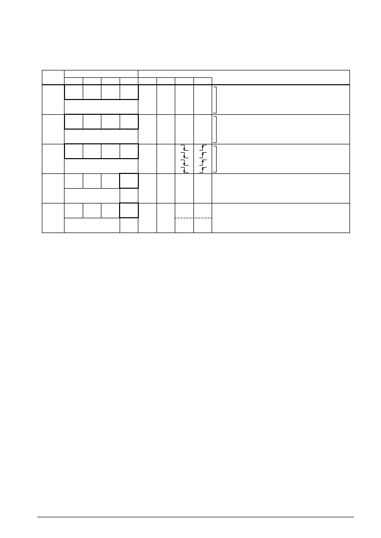
Table 4.4.4.1 shows the I/O addresses and the control bits for the input ports.
Table 4.4.4.1 Control bits of input ports
Address
Comment
D3
D2
Register
D1
D0
Name
Init 1
10
FF20H
SIK03
SIK02
SIK01
SIK00
R/W
SIK03
SIK02
SIK01
SIK00
0
Enable
Disable
K00–K03 interrupt selection register
FF21H
K03
K02
K01
K00
R
K03
K02
K01
K00
– 2
High
Low
K00–K03 input port data
FF22H
KCP03
KCP02
KCP01
KCP00
R/W
KCP03
KCP02
KCP01
KCP00
1
K00–K03 input comparison register
FFE4H
0
EIK0
RR/W
0 3
EIK0
– 2
0
Enable
Mask
Unused
Interrupt mask register (K00–K03)
FFF4H
000
IK0
RR/W
0 3
IK0
– 2
0
(R)
Yes
(W)
Reset
(R)
No
(W)
Invalid
Unused
Interrupt factor flag (K00–K03)
*1 Initial value at initial reset
*2 Not set in the circuit
*3 Constantly "0" when being read
K00–K03: K0 port input port data (FF21H)
Input data of the input port terminals can be read with these registers.
When "1" is read: High level
When "0" is read: Low level
Writing: Invalid
The reading is "1" when the terminal voltage of the four bits of the input ports (K00–K03) goes high
(VDD), and "0" when the voltage goes low (VSS).
These bits are dedicated for reading, so writing cannot be done.
SIK00–SIK03: K0 port interrupt selection register (FF20H)
Selects the ports to be used for the K00–K03 input interrupts.
When "1" is written: Enable
When "0" is written: Disable
Reading: Valid
Enables the interrupt for the input ports (K00–K03) for which "1" has been written into the interrupt
selection registers (SIK00–SIK03). The input port set for "0" does not affect the interrupt generation
condition.
At initial reset, these registers are set to "0".
KCP00–KCP03: K0 port input comparison register (FF22H)
Interrupt conditions for terminals K00–K03 can be set with these registers.
When "1" is written: Falling edge
When "0" is written: Rising edge
Reading: Valid
The interrupt conditions can be set for the rising or falling edge of input for each of the four bits (K00–
K03), through the input comparison registers (KCP00–KCP03).
相關(guān)PDF資料 |
PDF描述 |
|---|---|
| S1C63455D | 4-BIT, MROM, 4.1 MHz, MICROCONTROLLER, UUC105 |
| S1C63458F0A0100 | MICROCONTROLLER, PQFP144 |
| S1C63466D | 4-BIT, MROM, 4.1 MHz, MICROCONTROLLER, UUC140 |
| S1C63466F | 4-BIT, MROM, 4.1 MHz, MICROCONTROLLER, PQFP144 |
| S1C63567F0A0100 | MICROCONTROLLER, PQFP144 |
相關(guān)代理商/技術(shù)參數(shù) |
參數(shù)描述 |
|---|---|
| S1C63557D04Q000 | 制造商:Seiko Instruments Inc (SII) 功能描述:EPSON MCU 4BIT |
| S1C63567 | 制造商:EPSON 制造商全稱:EPSON 功能描述:4-bit Single Chip Microcomputer |
| S1C63616 | 制造商:EPSON 制造商全稱:EPSON 功能描述:4-bit Single Chip Microcomputer |
| S1C63632 | 制造商:EPSON 制造商全稱:EPSON 功能描述:4-bit Single Chip Microcomputer |
| S1C63653 | 制造商:EPSON 制造商全稱:EPSON 功能描述:CMOS 4-bit Single Chip Microcontroller |
發(fā)布緊急采購(gòu),3分鐘左右您將得到回復(fù)。