- 您現(xiàn)在的位置:買(mǎi)賣(mài)IC網(wǎng) > PDF目錄299581 > ORLI10G-2BM680 (LATTICE SEMICONDUCTOR CORP) FPGA, 1296 CLBS, 380000 GATES, PBGA680 PDF資料下載
參數(shù)資料
| 型號(hào): | ORLI10G-2BM680 |
| 廠(chǎng)商: | LATTICE SEMICONDUCTOR CORP |
| 元件分類(lèi): | FPGA |
| 英文描述: | FPGA, 1296 CLBS, 380000 GATES, PBGA680 |
| 封裝: | PLASTIC, BGA-680 |
| 文件頁(yè)數(shù): | 68/76頁(yè) |
| 文件大小: | 1222K |
| 代理商: | ORLI10G-2BM680 |
第1頁(yè)第2頁(yè)第3頁(yè)第4頁(yè)第5頁(yè)第6頁(yè)第7頁(yè)第8頁(yè)第9頁(yè)第10頁(yè)第11頁(yè)第12頁(yè)第13頁(yè)第14頁(yè)第15頁(yè)第16頁(yè)第17頁(yè)第18頁(yè)第19頁(yè)第20頁(yè)第21頁(yè)第22頁(yè)第23頁(yè)第24頁(yè)第25頁(yè)第26頁(yè)第27頁(yè)第28頁(yè)第29頁(yè)第30頁(yè)第31頁(yè)第32頁(yè)第33頁(yè)第34頁(yè)第35頁(yè)第36頁(yè)第37頁(yè)第38頁(yè)第39頁(yè)第40頁(yè)第41頁(yè)第42頁(yè)第43頁(yè)第44頁(yè)第45頁(yè)第46頁(yè)第47頁(yè)第48頁(yè)第49頁(yè)第50頁(yè)第51頁(yè)第52頁(yè)第53頁(yè)第54頁(yè)第55頁(yè)第56頁(yè)第57頁(yè)第58頁(yè)第59頁(yè)第60頁(yè)第61頁(yè)第62頁(yè)第63頁(yè)第64頁(yè)第65頁(yè)第66頁(yè)第67頁(yè)當(dāng)前第68頁(yè)第69頁(yè)第70頁(yè)第71頁(yè)第72頁(yè)第73頁(yè)第74頁(yè)第75頁(yè)第76頁(yè)
70
Lattice Semiconductor
Data Sheet
January 15, 2002
and ORLI12G Gbits/s Line Interface FPSC
ORCA ORLI10G Quad 2.5 Gbits/s, 10 Gbits/s
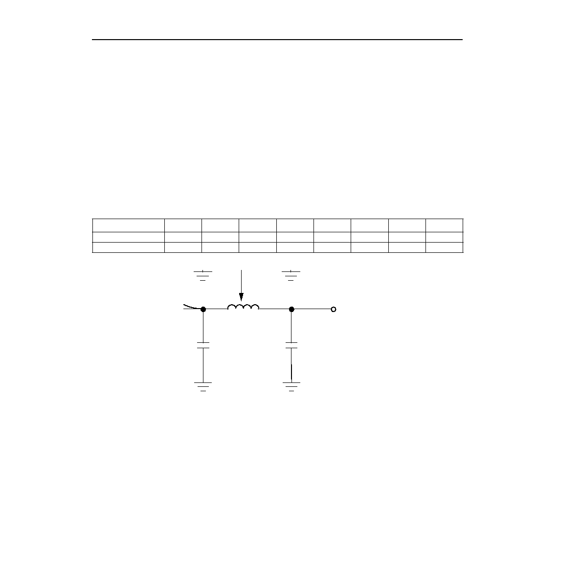
Package Parasitics
The electrical performance of an IC package, such as signal quality and noise sensitivity, is directly affected by the
package parasitics. Table 23 lists eight parasitics associated with the ORCA packages. These parasitics represent
the contributions of all components of a package, which include the bond wires, all internal package routing, and
the external leads.
Four inductances in nH are listed: LSW and LSL, the self-inductance of the lead; and LMW and LML, the mutual
inductance to the nearest neighbor lead. These parameters are important in determining ground bounce noise and
inductive crosstalk noise. Three capacitances in pF are listed: CM, the mutual capacitance of the lead to the near-
est neighbor lead; and C1 and C2, the total capacitance of the lead to all other leads (all other leads are assumed
to be grounded). These parameters are important in determining capacitive crosstalk and the capacitive loading
effect of the lead. Resistance values are in m.
The parasitic values in Table 23 are for the circuit model of bond wire and package lead parasitics. If the mutual
capacitance value is not used in the designer's model, then the value listed as mutual capacitance should be
added to each of the C1 and C2 capacitors.
Table 22. ORCA ORLI10G Package Parasitics
5-3862(C)r2
Figure 26. Package Parasitics
Package Type
LSW
LMW
RW
C1
C2
CM
LSL
LML
416-Pin PBGAM
3.52
0.80
235
0.40
1.0
0.25
1.5—5.0
0.5—1.30
680-Pin PBGAM
3.80
1.30
250
0.50
1.0
0.30
2.8—5.0
0.5—1.50
LSL
C2
C1
相關(guān)PDF資料 |
PDF描述 |
|---|---|
| ORLI10G-3BM416 | FPGA, 1296 CLBS, 380000 GATES, PBGA416 |
| ORLI10G-3BM680 | FPGA, 1296 CLBS, 380000 GATES, PBGA680 |
| ORLI10G1BM680-DB | FPGA, 1296 CLBS, 333000 GATES, PBGA680 |
| ORLI10G2BM680-DB | FPGA, 1296 CLBS, 333000 GATES, PBGA680 |
| ORLI10G3BM680-DB | FPGA, 1296 CLBS, 333000 GATES, PBGA680 |
相關(guān)代理商/技術(shù)參數(shù) |
參數(shù)描述 |
|---|---|
| ORLI10G-2BM680C | 功能描述:FPGA - 現(xiàn)場(chǎng)可編程門(mén)陣列 10368 LUT 316 I/O RoHS:否 制造商:Altera Corporation 系列:Cyclone V E 柵極數(shù)量: 邏輯塊數(shù)量:943 內(nèi)嵌式塊RAM - EBR:1956 kbit 輸入/輸出端數(shù)量:128 最大工作頻率:800 MHz 工作電源電壓:1.1 V 最大工作溫度:+ 70 C 安裝風(fēng)格:SMD/SMT 封裝 / 箱體:FBGA-256 |
| ORLI10G-2BM680I | 功能描述:FPGA - 現(xiàn)場(chǎng)可編程門(mén)陣列 10368 LUT 316 I/O RoHS:否 制造商:Altera Corporation 系列:Cyclone V E 柵極數(shù)量: 邏輯塊數(shù)量:943 內(nèi)嵌式塊RAM - EBR:1956 kbit 輸入/輸出端數(shù)量:128 最大工作頻率:800 MHz 工作電源電壓:1.1 V 最大工作溫度:+ 70 C 安裝風(fēng)格:SMD/SMT 封裝 / 箱體:FBGA-256 |
| ORLI10G-2BMN680C | 功能描述:FPGA - 現(xiàn)場(chǎng)可編程門(mén)陣列 10368 LUT 316 I/O RoHS:否 制造商:Altera Corporation 系列:Cyclone V E 柵極數(shù)量: 邏輯塊數(shù)量:943 內(nèi)嵌式塊RAM - EBR:1956 kbit 輸入/輸出端數(shù)量:128 最大工作頻率:800 MHz 工作電源電壓:1.1 V 最大工作溫度:+ 70 C 安裝風(fēng)格:SMD/SMT 封裝 / 箱體:FBGA-256 |
| ORLI10G-2BMN680I | 功能描述:FPGA - 現(xiàn)場(chǎng)可編程門(mén)陣列 10368 LUT 316 I/O RoHS:否 制造商:Altera Corporation 系列:Cyclone V E 柵極數(shù)量: 邏輯塊數(shù)量:943 內(nèi)嵌式塊RAM - EBR:1956 kbit 輸入/輸出端數(shù)量:128 最大工作頻率:800 MHz 工作電源電壓:1.1 V 最大工作溫度:+ 70 C 安裝風(fēng)格:SMD/SMT 封裝 / 箱體:FBGA-256 |
| ORLI10G-3BM680C | 功能描述:FPGA - 現(xiàn)場(chǎng)可編程門(mén)陣列 10368 LUT 316 I/O RoHS:否 制造商:Altera Corporation 系列:Cyclone V E 柵極數(shù)量: 邏輯塊數(shù)量:943 內(nèi)嵌式塊RAM - EBR:1956 kbit 輸入/輸出端數(shù)量:128 最大工作頻率:800 MHz 工作電源電壓:1.1 V 最大工作溫度:+ 70 C 安裝風(fēng)格:SMD/SMT 封裝 / 箱體:FBGA-256 |
發(fā)布緊急采購(gòu),3分鐘左右您將得到回復(fù)。