- 您現(xiàn)在的位置:買賣IC網(wǎng) > PDF目錄299581 > ORLI10G-2BM416 (LATTICE SEMICONDUCTOR CORP) FPGA, 1296 CLBS, 380000 GATES, PBGA416 PDF資料下載
參數(shù)資料
| 型號(hào): | ORLI10G-2BM416 |
| 廠商: | LATTICE SEMICONDUCTOR CORP |
| 元件分類: | FPGA |
| 英文描述: | FPGA, 1296 CLBS, 380000 GATES, PBGA416 |
| 封裝: | PLASTIC, BGA-416 |
| 文件頁數(shù): | 27/76頁 |
| 文件大小: | 1222K |
| 代理商: | ORLI10G-2BM416 |
第1頁第2頁第3頁第4頁第5頁第6頁第7頁第8頁第9頁第10頁第11頁第12頁第13頁第14頁第15頁第16頁第17頁第18頁第19頁第20頁第21頁第22頁第23頁第24頁第25頁第26頁當(dāng)前第27頁第28頁第29頁第30頁第31頁第32頁第33頁第34頁第35頁第36頁第37頁第38頁第39頁第40頁第41頁第42頁第43頁第44頁第45頁第46頁第47頁第48頁第49頁第50頁第51頁第52頁第53頁第54頁第55頁第56頁第57頁第58頁第59頁第60頁第61頁第62頁第63頁第64頁第65頁第66頁第67頁第68頁第69頁第70頁第71頁第72頁第73頁第74頁第75頁第76頁
Lattice Semiconductor
33
Data Sheet
January 15, 2002
and ORLI12G Gbits/s Line Interface FPSC
ORCA ORLI10G Quad 2.5 Gbits/s, 10 Gbits/s
Line Interface Circuit Specications
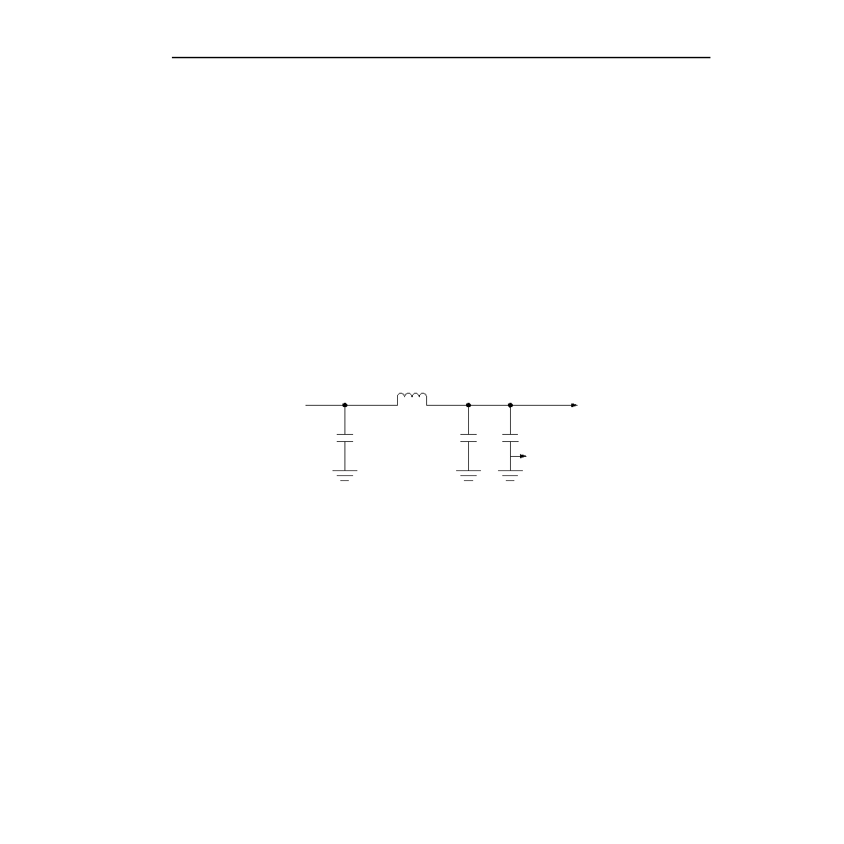
Power Supply Decoupling LC Circuit
The 622 MHz—850 MHz line interface macro contains both analog and digital circuitry. The line interface function,
for example, is implemented as primarily a digital function, but it relies on a conventional analog phase-locked loop
to provide its divided clocks. The internal analog phase-locked loop contains a voltage-controlled oscillator. This
circuit will be sensitive to digital noise generated from the rapid switching transients associated with internal logic
gates and parasitic inductive elements. Generated noise that contains frequency components beyond the band-
width of the internal phase-locked loop (about 3 MHz) will not be attenuated by the phase-locked loop and will
impact bit error rate directly. Thus, separate power supply pins are provided for these critical analog circuit ele-
ments.
Additional power supply ltering in the form of an LC pi lter section will be used between the power supply source
and these device pins as shown in Figure 16. The corner frequency of the LC lter is chosen based on the power
supply switching frequency, which is between 100 kHz and 300 kHz in most applications.
Capacitors C1 and C2 are large electrolytic capacitors to provide the basic cut-off frequency of the LC lter. For
example, the cut-off frequency of the combination of these elements might fall between 5 kHz and 50 kHz. Capac-
itor C3 is a smaller ceramic capacitor designed to provide a low-impedance path for a wide range of high-fre-
quency signals at the analog power supply pins of the device. The physical location of capacitor C3 must be as
close to the device lead as possible. Multiple instances of capacitors C3 can be used if necessary. The recom-
mended lter for the HSI macro is shown below: L = 4.7 H, RL = 1 , C1 = 0.01 F, C2 = 0.01 F, C3 = 4.7 F.
5-9344(F).a
Figure 16. Sample Power Supply Filter Network for Analog LI Power Supply Pins
C2
+
C3
+
TO DEVICE
VDDA_[7:4]
VSSA_[7:4]
C1
+
FROM POWER
SUPPLY SOURCE
L
相關(guān)PDF資料 |
PDF描述 |
|---|---|
| ORLI10G-2BM680 | FPGA, 1296 CLBS, 380000 GATES, PBGA680 |
| ORLI10G-3BM416 | FPGA, 1296 CLBS, 380000 GATES, PBGA416 |
| ORLI10G-3BM680 | FPGA, 1296 CLBS, 380000 GATES, PBGA680 |
| ORLI10G1BM680-DB | FPGA, 1296 CLBS, 333000 GATES, PBGA680 |
| ORLI10G2BM680-DB | FPGA, 1296 CLBS, 333000 GATES, PBGA680 |
相關(guān)代理商/技術(shù)參數(shù) |
參數(shù)描述 |
|---|---|
| ORLI10G-2BM680C | 功能描述:FPGA - 現(xiàn)場(chǎng)可編程門陣列 10368 LUT 316 I/O RoHS:否 制造商:Altera Corporation 系列:Cyclone V E 柵極數(shù)量: 邏輯塊數(shù)量:943 內(nèi)嵌式塊RAM - EBR:1956 kbit 輸入/輸出端數(shù)量:128 最大工作頻率:800 MHz 工作電源電壓:1.1 V 最大工作溫度:+ 70 C 安裝風(fēng)格:SMD/SMT 封裝 / 箱體:FBGA-256 |
| ORLI10G-2BM680I | 功能描述:FPGA - 現(xiàn)場(chǎng)可編程門陣列 10368 LUT 316 I/O RoHS:否 制造商:Altera Corporation 系列:Cyclone V E 柵極數(shù)量: 邏輯塊數(shù)量:943 內(nèi)嵌式塊RAM - EBR:1956 kbit 輸入/輸出端數(shù)量:128 最大工作頻率:800 MHz 工作電源電壓:1.1 V 最大工作溫度:+ 70 C 安裝風(fēng)格:SMD/SMT 封裝 / 箱體:FBGA-256 |
| ORLI10G-2BMN680C | 功能描述:FPGA - 現(xiàn)場(chǎng)可編程門陣列 10368 LUT 316 I/O RoHS:否 制造商:Altera Corporation 系列:Cyclone V E 柵極數(shù)量: 邏輯塊數(shù)量:943 內(nèi)嵌式塊RAM - EBR:1956 kbit 輸入/輸出端數(shù)量:128 最大工作頻率:800 MHz 工作電源電壓:1.1 V 最大工作溫度:+ 70 C 安裝風(fēng)格:SMD/SMT 封裝 / 箱體:FBGA-256 |
| ORLI10G-2BMN680I | 功能描述:FPGA - 現(xiàn)場(chǎng)可編程門陣列 10368 LUT 316 I/O RoHS:否 制造商:Altera Corporation 系列:Cyclone V E 柵極數(shù)量: 邏輯塊數(shù)量:943 內(nèi)嵌式塊RAM - EBR:1956 kbit 輸入/輸出端數(shù)量:128 最大工作頻率:800 MHz 工作電源電壓:1.1 V 最大工作溫度:+ 70 C 安裝風(fēng)格:SMD/SMT 封裝 / 箱體:FBGA-256 |
| ORLI10G-3BM680C | 功能描述:FPGA - 現(xiàn)場(chǎng)可編程門陣列 10368 LUT 316 I/O RoHS:否 制造商:Altera Corporation 系列:Cyclone V E 柵極數(shù)量: 邏輯塊數(shù)量:943 內(nèi)嵌式塊RAM - EBR:1956 kbit 輸入/輸出端數(shù)量:128 最大工作頻率:800 MHz 工作電源電壓:1.1 V 最大工作溫度:+ 70 C 安裝風(fēng)格:SMD/SMT 封裝 / 箱體:FBGA-256 |
發(fā)布緊急采購,3分鐘左右您將得到回復(fù)。