- 您現(xiàn)在的位置:買賣IC網(wǎng) > PDF目錄383723 > OR3TP12-6BA256I Single 2.3V 10 MHZ OP, -40C to +125C, 14-SOIC 150mil, TUBE PDF資料下載
參數(shù)資料
| 型號: | OR3TP12-6BA256I |
| 英文描述: | Single 2.3V 10 MHZ OP, -40C to +125C, 14-SOIC 150mil, TUBE |
| 中文描述: | 用戶可編程ASIC的特殊功能 |
| 文件頁數(shù): | 98/128頁 |
| 文件大?。?/td> | 2450K |
| 代理商: | OR3TP12-6BA256I |
第1頁第2頁第3頁第4頁第5頁第6頁第7頁第8頁第9頁第10頁第11頁第12頁第13頁第14頁第15頁第16頁第17頁第18頁第19頁第20頁第21頁第22頁第23頁第24頁第25頁第26頁第27頁第28頁第29頁第30頁第31頁第32頁第33頁第34頁第35頁第36頁第37頁第38頁第39頁第40頁第41頁第42頁第43頁第44頁第45頁第46頁第47頁第48頁第49頁第50頁第51頁第52頁第53頁第54頁第55頁第56頁第57頁第58頁第59頁第60頁第61頁第62頁第63頁第64頁第65頁第66頁第67頁第68頁第69頁第70頁第71頁第72頁第73頁第74頁第75頁第76頁第77頁第78頁第79頁第80頁第81頁第82頁第83頁第84頁第85頁第86頁第87頁第88頁第89頁第90頁第91頁第92頁第93頁第94頁第95頁第96頁第97頁當前第98頁第99頁第100頁第101頁第102頁第103頁第104頁第105頁第106頁第107頁第108頁第109頁第110頁第111頁第112頁第113頁第114頁第115頁第116頁第117頁第118頁第119頁第120頁第121頁第122頁第123頁第124頁第125頁第126頁第127頁第128頁
ORCAOR3TP12 FPSC
Embedded Master/Target PCI Interface
Data Sheet
March 2000
98
L Lucent Technologies Inc.
Timing Characteristics
(continued)
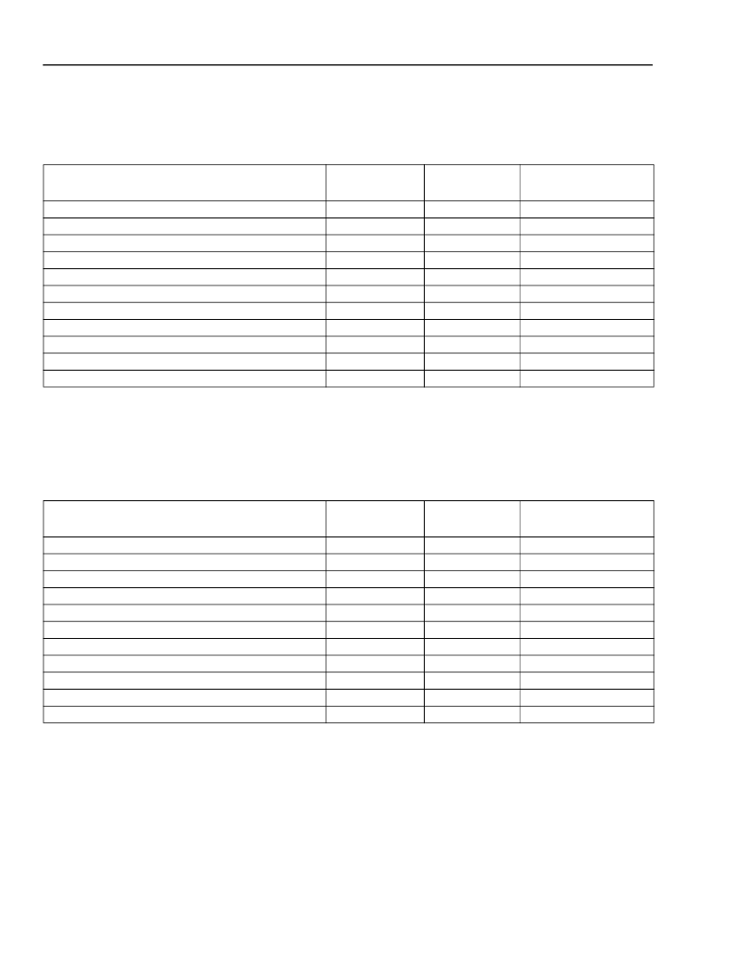
Table 39. OR3TP12 FPGA Side Interface Input Setup Delays, pciclk Synchronous Signals
OR3TP12 Commercial: V
DD
= 3.0 V to 3.6 V, 0 °C < T
A
< 70 °C.
Note: The input setup parameters are measured from the
pciclk
clock output pin on the FPGA side, excluding the interbufs, which traverse the
ASIC/FPGA boundary. The ORCAFoundry static analysis tool, trace, accounts for clock skew and interbuf delays on the clock and data
paths.
Table 40. OR3TP12 FPGA Side Interface Input Setup Delays, fclk Synchronous Signals
OR3TP12 Commercial: V
DD
= 3.0 V to 3.6 V, 0 °C < T
A
< 70 °C.
Note: The input setup parameters are measured from the
fclk1
and
fclk2
clock input pins on the FPGA side, excluding the interbufs, which
traverse the ASIC/FPGA boundary. The ORCA Foundry static analysis tool, trace, accounts for clock skew and interbuf delays on the
clock and data paths.
Description
(TI = 85 °C, V
DD
= min, V
DD
2 = min)
fpga_mbusyn
deltrn
mwpcihold
mr_mstopburstn
t_abort
t_retryn
twburstpendn
trpcihold
trburstpendn
fpga_syserror
cfgshiftenn
Min
Max
Unit
0
0
—
—
—
—
—
—
—
—
—
—
—
ns
ns
ns
ns
ns
ns
ns
ns
ns
ns
ns
3.943
0
1.197
0.795
0
0.693
0
0
0
Description
(TI = 85 °C, V
DD
= min, V
DD
2 = min)
Min
Max
Unit
maenn
mwdataenn
datafmfpga[31:0]
(dual-port mode)
datafmfpgax[3:0]
(dual-port mode)
mwdata[17:0]
(quad-port mode)
trdata[17:0]
(quad-port mode)
mwlastcycn
mrdataenn
taenn
twdataenn
trdataenn
6.426
6.452
7.344
5.226
7.205
7.344
6.680
5.371
5.048
5.099
5.919
—
—
—
—
—
—
—
—
—
—
—
ns
ns
ns
ns
ns
ns
ns
ns
ns
ns
ns
相關PDF資料 |
PDF描述 |
|---|---|
| OR3TP12-6BA352 | Quad 2.3V 10 MHz OP, I temp, -40C to +85C, 14-PDIP, TUBE |
| OR3TP12-6BA352I | Quad 2.3V 10 MHz OP, I temp, -40C to +85C, 14-TSSOP, TUBE |
| OR3TP12-6PS240 | Single 2.3V 10 MHZ OP, -40C to +125C, 14-SOIC 150mil, T/R |
| OR3TP12-6PS240I | Quad 2.3V 10 MHz OP, I temp, -40C to +85C, 14-SOIC 150mil, T/R |
| OR3TP12 | Field-Programmable System Chip (FPSC) Embedded Master/Target PCI Interface |
相關代理商/技術(shù)參數(shù) |
參數(shù)描述 |
|---|---|
| OR3TP126BA256I-DB | 功能描述:FPGA - 現(xiàn)場可編程門陣列 2016 LUT 187 I/O RoHS:否 制造商:Altera Corporation 系列:Cyclone V E 柵極數(shù)量: 邏輯塊數(shù)量:943 內(nèi)嵌式塊RAM - EBR:1956 kbit 輸入/輸出端數(shù)量:128 最大工作頻率:800 MHz 工作電源電壓:1.1 V 最大工作溫度:+ 70 C 安裝風格:SMD/SMT 封裝 / 箱體:FBGA-256 |
| OR3TP12-6BA352 | 制造商:未知廠家 制造商全稱:未知廠家 功能描述:User Programmable Special Function ASIC |
| OR3TP126BA352-DB | 功能描述:FPGA - 現(xiàn)場可編程門陣列 2016 LUT 187 I/O RoHS:否 制造商:Altera Corporation 系列:Cyclone V E 柵極數(shù)量: 邏輯塊數(shù)量:943 內(nèi)嵌式塊RAM - EBR:1956 kbit 輸入/輸出端數(shù)量:128 最大工作頻率:800 MHz 工作電源電壓:1.1 V 最大工作溫度:+ 70 C 安裝風格:SMD/SMT 封裝 / 箱體:FBGA-256 |
| OR3TP12-6BA352I | 制造商:未知廠家 制造商全稱:未知廠家 功能描述:User Programmable Special Function ASIC |
| OR3TP126BAN256-DB | 制造商:Lattice Semiconductor Corporation 功能描述: |
發(fā)布緊急采購,3分鐘左右您將得到回復。