- 您現(xiàn)在的位置:買賣IC網(wǎng) > PDF目錄383723 > OR3TP12-6BA256I Single 2.3V 10 MHZ OP, -40C to +125C, 14-SOIC 150mil, TUBE PDF資料下載
參數(shù)資料
| 型號(hào): | OR3TP12-6BA256I |
| 英文描述: | Single 2.3V 10 MHZ OP, -40C to +125C, 14-SOIC 150mil, TUBE |
| 中文描述: | 用戶可編程ASIC的特殊功能 |
| 文件頁(yè)數(shù): | 103/128頁(yè) |
| 文件大?。?/td> | 2450K |
| 代理商: | OR3TP12-6BA256I |
第1頁(yè)第2頁(yè)第3頁(yè)第4頁(yè)第5頁(yè)第6頁(yè)第7頁(yè)第8頁(yè)第9頁(yè)第10頁(yè)第11頁(yè)第12頁(yè)第13頁(yè)第14頁(yè)第15頁(yè)第16頁(yè)第17頁(yè)第18頁(yè)第19頁(yè)第20頁(yè)第21頁(yè)第22頁(yè)第23頁(yè)第24頁(yè)第25頁(yè)第26頁(yè)第27頁(yè)第28頁(yè)第29頁(yè)第30頁(yè)第31頁(yè)第32頁(yè)第33頁(yè)第34頁(yè)第35頁(yè)第36頁(yè)第37頁(yè)第38頁(yè)第39頁(yè)第40頁(yè)第41頁(yè)第42頁(yè)第43頁(yè)第44頁(yè)第45頁(yè)第46頁(yè)第47頁(yè)第48頁(yè)第49頁(yè)第50頁(yè)第51頁(yè)第52頁(yè)第53頁(yè)第54頁(yè)第55頁(yè)第56頁(yè)第57頁(yè)第58頁(yè)第59頁(yè)第60頁(yè)第61頁(yè)第62頁(yè)第63頁(yè)第64頁(yè)第65頁(yè)第66頁(yè)第67頁(yè)第68頁(yè)第69頁(yè)第70頁(yè)第71頁(yè)第72頁(yè)第73頁(yè)第74頁(yè)第75頁(yè)第76頁(yè)第77頁(yè)第78頁(yè)第79頁(yè)第80頁(yè)第81頁(yè)第82頁(yè)第83頁(yè)第84頁(yè)第85頁(yè)第86頁(yè)第87頁(yè)第88頁(yè)第89頁(yè)第90頁(yè)第91頁(yè)第92頁(yè)第93頁(yè)第94頁(yè)第95頁(yè)第96頁(yè)第97頁(yè)第98頁(yè)第99頁(yè)第100頁(yè)第101頁(yè)第102頁(yè)當(dāng)前第103頁(yè)第104頁(yè)第105頁(yè)第106頁(yè)第107頁(yè)第108頁(yè)第109頁(yè)第110頁(yè)第111頁(yè)第112頁(yè)第113頁(yè)第114頁(yè)第115頁(yè)第116頁(yè)第117頁(yè)第118頁(yè)第119頁(yè)第120頁(yè)第121頁(yè)第122頁(yè)第123頁(yè)第124頁(yè)第125頁(yè)第126頁(yè)第127頁(yè)第128頁(yè)
Lucent Technologies Inc.
Lucent Technologies Inc.
103
Data Sheet
March 2000
ORCA OR3TP12 FPSC
Embedded Master/Target PCI Interface
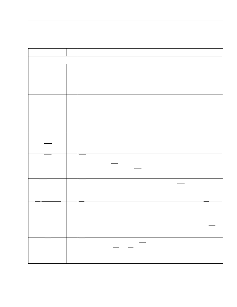
Table 41. FPGA Common-Function Pin Descriptions
(continued)
** The ORCA Series 3 FPGA data sheet contains more information on how to control these signals during start-up. The timing of DONE release
is controlled by one set of bit stream options, and the timing of the simultaneous release of all other configuration pins (and the activation of all
user I/Os) is controlled by a second set of options.
Symbol
I/O
Description
Special-Purpose Pins
(continued)
TDI, TCK, TMS
I
I/O
O
If boundary scan is used, these pins are test data in, test clock, and test mode select
inputs. If boundary scan is not selected, all boundary-scan functions are inhibited
once configuration is complete. Even if boundary scan is not used, either TCK or
TMS must be held at logic one during configuration. Each pin has a pull-up enabled
during configuration.
After configuration, these pins are user-programmable I/O.*
During configuration in peripheral mode, RDY/RCLK indicates another byte can be
written to the FPGA. If a read operation is done when the device is selected, the
same status is also available on D7 in asynchronous peripheral mode.
During the Master parallel configuration mode, RCLK is a read output signal to an
external memory. This output is not normally used.
In i960microprocessor mode, this pin acts as the address latch enable (ALE) input.
After configuration, if the MPI is not used, this pin is a user-programmable I/O pin.*
High during configuration is output high until configuration is complete. It is used as
a control output indicating that configuration is not complete.
Low during configuration is output low until configuration is complete. It is used as a
control output indicating that configuration is not complete.
INIT is a bidirectional signal before and during configuration. During configuration, a
pull-up is enabled, but an external pull-up resistor is recommended. As an active-low
open-drain output, INIT is held low during power stabilization and internal clearing of
memory. As an active-low input, INIT holds the FPGA in the wait-state before the
start of configuration.
CS0 and CS1 are used in the asynchronous peripheral, slave parallel, and micropro-
cessor configuration modes. The FPGA is selected when CS0 is low and CS1 is
high. During configuration, a pull-up is enabled.
RDY/RCLK/
MPI_ALE
O
I
I/O
O
HDC
LDC
O
INIT
I/O
CS0, CS1
I
I/O
I
After configuration, these pins are user-programmable I/O pins.*
RD is used in the asynchronous peripheral configuration mode. A low on RD
changes D7 into a status output. As a status indication, a high indicates ready, and a
low indicates busy. WR and RD should not be used simultaneously. If they are, the
write strobe overrides.
This pin is also used as the microprocessor interface (MPI) data transfer strobe. For
PowerPC it is the transfer start (TS). For i960, it is the address/data strobe (
ads
).
After configuration, if the MPI is not used, this pin is a user-programmable I/O pin.*
WR is used in the asynchronous peripheral configuration mode. When the FPGA is
selected, a low on the write strobe, WR, loads the data on D[7:0] inputs into an
internal data buffer. WR and RD should not be used simultaneously. If they are, the
write strobe overrides.
After configuration, this pin is a user-programmable I/O pin.*
RD/MPI_STRB
I
I/O
I
WR
I/O
Pin Information
(continued)
相關(guān)PDF資料 |
PDF描述 |
|---|---|
| OR3TP12-6BA352 | Quad 2.3V 10 MHz OP, I temp, -40C to +85C, 14-PDIP, TUBE |
| OR3TP12-6BA352I | Quad 2.3V 10 MHz OP, I temp, -40C to +85C, 14-TSSOP, TUBE |
| OR3TP12-6PS240 | Single 2.3V 10 MHZ OP, -40C to +125C, 14-SOIC 150mil, T/R |
| OR3TP12-6PS240I | Quad 2.3V 10 MHz OP, I temp, -40C to +85C, 14-SOIC 150mil, T/R |
| OR3TP12 | Field-Programmable System Chip (FPSC) Embedded Master/Target PCI Interface |
相關(guān)代理商/技術(shù)參數(shù) |
參數(shù)描述 |
|---|---|
| OR3TP126BA256I-DB | 功能描述:FPGA - 現(xiàn)場(chǎng)可編程門陣列 2016 LUT 187 I/O RoHS:否 制造商:Altera Corporation 系列:Cyclone V E 柵極數(shù)量: 邏輯塊數(shù)量:943 內(nèi)嵌式塊RAM - EBR:1956 kbit 輸入/輸出端數(shù)量:128 最大工作頻率:800 MHz 工作電源電壓:1.1 V 最大工作溫度:+ 70 C 安裝風(fēng)格:SMD/SMT 封裝 / 箱體:FBGA-256 |
| OR3TP12-6BA352 | 制造商:未知廠家 制造商全稱:未知廠家 功能描述:User Programmable Special Function ASIC |
| OR3TP126BA352-DB | 功能描述:FPGA - 現(xiàn)場(chǎng)可編程門陣列 2016 LUT 187 I/O RoHS:否 制造商:Altera Corporation 系列:Cyclone V E 柵極數(shù)量: 邏輯塊數(shù)量:943 內(nèi)嵌式塊RAM - EBR:1956 kbit 輸入/輸出端數(shù)量:128 最大工作頻率:800 MHz 工作電源電壓:1.1 V 最大工作溫度:+ 70 C 安裝風(fēng)格:SMD/SMT 封裝 / 箱體:FBGA-256 |
| OR3TP12-6BA352I | 制造商:未知廠家 制造商全稱:未知廠家 功能描述:User Programmable Special Function ASIC |
| OR3TP126BAN256-DB | 制造商:Lattice Semiconductor Corporation 功能描述: |
發(fā)布緊急采購(gòu),3分鐘左右您將得到回復(fù)。