- 您現(xiàn)在的位置:買賣IC網(wǎng) > PDF目錄299575 > OR3T307S240-DB (LATTICE SEMICONDUCTOR CORP) FPGA, 196 CLBS, 48000 GATES, PQFP240 PDF資料下載
參數(shù)資料
| 型號(hào): | OR3T307S240-DB |
| 廠商: | LATTICE SEMICONDUCTOR CORP |
| 元件分類: | FPGA |
| 英文描述: | FPGA, 196 CLBS, 48000 GATES, PQFP240 |
| 封裝: | PLASTIC, SQFP-240 |
| 文件頁數(shù): | 56/203頁 |
| 文件大小: | 1368K |
| 代理商: | OR3T307S240-DB |
第1頁第2頁第3頁第4頁第5頁第6頁第7頁第8頁第9頁第10頁第11頁第12頁第13頁第14頁第15頁第16頁第17頁第18頁第19頁第20頁第21頁第22頁第23頁第24頁第25頁第26頁第27頁第28頁第29頁第30頁第31頁第32頁第33頁第34頁第35頁第36頁第37頁第38頁第39頁第40頁第41頁第42頁第43頁第44頁第45頁第46頁第47頁第48頁第49頁第50頁第51頁第52頁第53頁第54頁第55頁當(dāng)前第56頁第57頁第58頁第59頁第60頁第61頁第62頁第63頁第64頁第65頁第66頁第67頁第68頁第69頁第70頁第71頁第72頁第73頁第74頁第75頁第76頁第77頁第78頁第79頁第80頁第81頁第82頁第83頁第84頁第85頁第86頁第87頁第88頁第89頁第90頁第91頁第92頁第93頁第94頁第95頁第96頁第97頁第98頁第99頁第100頁第101頁第102頁第103頁第104頁第105頁第106頁第107頁第108頁第109頁第110頁第111頁第112頁第113頁第114頁第115頁第116頁第117頁第118頁第119頁第120頁第121頁第122頁第123頁第124頁第125頁第126頁第127頁第128頁第129頁第130頁第131頁第132頁第133頁第134頁第135頁第136頁第137頁第138頁第139頁第140頁第141頁第142頁第143頁第144頁第145頁第146頁第147頁第148頁第149頁第150頁第151頁第152頁第153頁第154頁第155頁第156頁第157頁第158頁第159頁第160頁第161頁第162頁第163頁第164頁第165頁第166頁第167頁第168頁第169頁第170頁第171頁第172頁第173頁第174頁第175頁第176頁第177頁第178頁第179頁第180頁第181頁第182頁第183頁第184頁第185頁第186頁第187頁第188頁第189頁第190頁第191頁第192頁第193頁第194頁第195頁第196頁第197頁第198頁第199頁第200頁第201頁第202頁第203頁
Lattice Semiconductor
149
Data Sheet
November 2006
ORCA Series 3C and 3T FPGAs
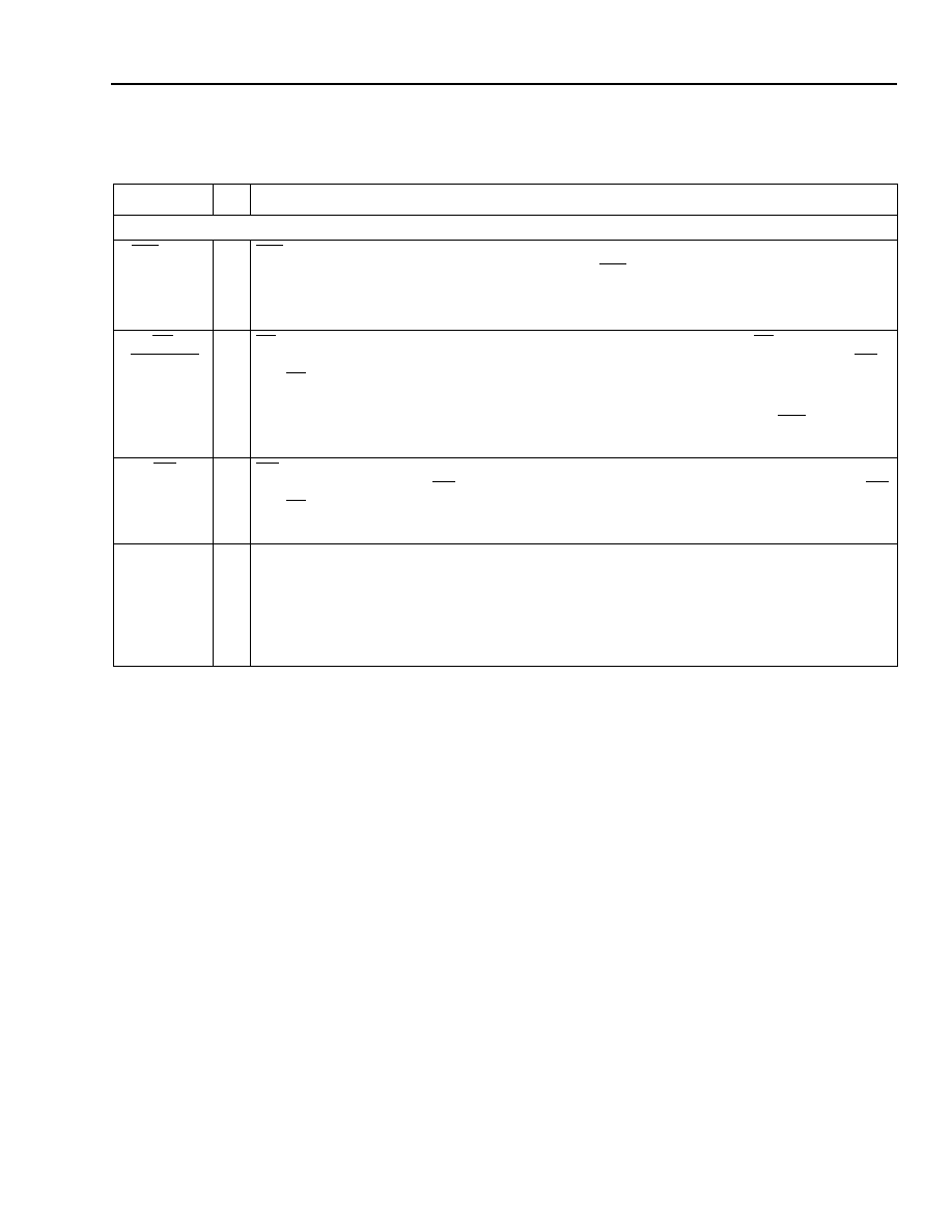
Special-Purpose Pins
(continued)
CS0
, CS1
I
I/O
CS0
and CS1 are used in the asynchronous peripheral, slave parallel, and microprocessor
conguration modes. The FPGA is selected when CS0 is low and CS1 is high. During cong-
uration, a pull-up is enabled.
After conguration, these pins are user-programmable I/O pins (see Note).
RD
/
MPI_STRB
I
I/O
RD
is used in the asynchronous peripheral conguration mode. A low on RD changes D7 into
a status output. As a status indication, a high indicates ready, and a low indicates busy. WR
and RD should not be used simultaneously. If they are, the write strobe overrides.
This pin is also used as the microprocessor interface (MPI) data transfer strobe. For
PowerPC, it is the transfer start (TS). For i960, it is the address/data strobe (ADS).
After conguration, if the MPI is not used, this pin is a user-programmable I/O pin (see Note).
WR
I
I/O
WR
is used in the asynchronous peripheral conguration mode. When the FPGA is selected,
a low on the write strobe, WR, loads the data on D[7:0] inputs into an internal data buffer. WR
and RD should not be used simultaneously. If they are, the write strobe overrides.
After conguration, this pin is a user-programmable I/O pin (see Note).
A[17:0]
O
I/O
During master parallel conguration mode, A[17:0] address the conguration EPROM. In
microprocessor interface (MPI) mode, many of the A[n] pins have alternate uses as described
below. See the Special Function Blocks section for more MPI information. During congura-
tion, if not in master parallel or an MPI conguration mode, these pins are 3-stated with a pull-
up enabled.
After conguration, the pins are user-programmable I/O pins (see Note).
Pin Information (continued)
Table 67. Pin Descriptions (continued)
Symbol
I/O
Description
Note: The FPGA States of Operation section contains more information on how to control these signals during start-up. The timing of DONE
release is controlled by one set of bit stream options, and the timing of the simultaneous release of all other conguration pins (and the
activation of all user I/Os) is controlled by a second set of options.
Select
devices
have
been
discontinued.
See
Ordering
Information
section
for
product
status.
相關(guān)PDF資料 |
PDF描述 |
|---|---|
| OR3T556PS240-DB | FPGA, 324 CLBS, 80000 GATES, PQFP240 |
| OR3T806PS240-DB | FPGA, 484 CLBS, 116000 GATES, PQFP240 |
| OR3T807PS240-DB | FPGA, 484 CLBS, 116000 GATES, PQFP240 |
| OR3T55-4BA256I | FPGA, 324 CLBS, 40000 GATES, 80 MHz, PBGA256 |
| OR3T55-4BA256 | FPGA, 324 CLBS, 40000 GATES, 80 MHz, PBGA256 |
相關(guān)代理商/技術(shù)參數(shù) |
參數(shù)描述 |
|---|---|
| OR3T30-7S240I | 制造商:未知廠家 制造商全稱:未知廠家 功能描述:Field Programmable Gate Array (FPGA) |
| OR3T55 | 制造商:AGERE 制造商全稱:AGERE 功能描述:3C and 3T Field-Programmable Gate Arrays |
| OR3T55-4BA256I | 制造商:未知廠家 制造商全稱:未知廠家 功能描述:Field Programmable Gate Array (FPGA) |
| OR3T55-4PS208I | 制造商:未知廠家 制造商全稱:未知廠家 功能描述:Field Programmable Gate Array (FPGA) |
| OR3T55-4PS240I | 制造商:未知廠家 制造商全稱:未知廠家 功能描述:Field Programmable Gate Array (FPGA) |
發(fā)布緊急采購(gòu),3分鐘左右您將得到回復(fù)。