- 您現(xiàn)在的位置:買(mǎi)賣(mài)IC網(wǎng) > PDF目錄299575 > OR3T307S240-DB (LATTICE SEMICONDUCTOR CORP) FPGA, 196 CLBS, 48000 GATES, PQFP240 PDF資料下載
參數(shù)資料
| 型號(hào): | OR3T307S240-DB |
| 廠商: | LATTICE SEMICONDUCTOR CORP |
| 元件分類(lèi): | FPGA |
| 英文描述: | FPGA, 196 CLBS, 48000 GATES, PQFP240 |
| 封裝: | PLASTIC, SQFP-240 |
| 文件頁(yè)數(shù): | 12/203頁(yè) |
| 文件大小: | 1368K |
| 代理商: | OR3T307S240-DB |
第1頁(yè)第2頁(yè)第3頁(yè)第4頁(yè)第5頁(yè)第6頁(yè)第7頁(yè)第8頁(yè)第9頁(yè)第10頁(yè)第11頁(yè)當(dāng)前第12頁(yè)第13頁(yè)第14頁(yè)第15頁(yè)第16頁(yè)第17頁(yè)第18頁(yè)第19頁(yè)第20頁(yè)第21頁(yè)第22頁(yè)第23頁(yè)第24頁(yè)第25頁(yè)第26頁(yè)第27頁(yè)第28頁(yè)第29頁(yè)第30頁(yè)第31頁(yè)第32頁(yè)第33頁(yè)第34頁(yè)第35頁(yè)第36頁(yè)第37頁(yè)第38頁(yè)第39頁(yè)第40頁(yè)第41頁(yè)第42頁(yè)第43頁(yè)第44頁(yè)第45頁(yè)第46頁(yè)第47頁(yè)第48頁(yè)第49頁(yè)第50頁(yè)第51頁(yè)第52頁(yè)第53頁(yè)第54頁(yè)第55頁(yè)第56頁(yè)第57頁(yè)第58頁(yè)第59頁(yè)第60頁(yè)第61頁(yè)第62頁(yè)第63頁(yè)第64頁(yè)第65頁(yè)第66頁(yè)第67頁(yè)第68頁(yè)第69頁(yè)第70頁(yè)第71頁(yè)第72頁(yè)第73頁(yè)第74頁(yè)第75頁(yè)第76頁(yè)第77頁(yè)第78頁(yè)第79頁(yè)第80頁(yè)第81頁(yè)第82頁(yè)第83頁(yè)第84頁(yè)第85頁(yè)第86頁(yè)第87頁(yè)第88頁(yè)第89頁(yè)第90頁(yè)第91頁(yè)第92頁(yè)第93頁(yè)第94頁(yè)第95頁(yè)第96頁(yè)第97頁(yè)第98頁(yè)第99頁(yè)第100頁(yè)第101頁(yè)第102頁(yè)第103頁(yè)第104頁(yè)第105頁(yè)第106頁(yè)第107頁(yè)第108頁(yè)第109頁(yè)第110頁(yè)第111頁(yè)第112頁(yè)第113頁(yè)第114頁(yè)第115頁(yè)第116頁(yè)第117頁(yè)第118頁(yè)第119頁(yè)第120頁(yè)第121頁(yè)第122頁(yè)第123頁(yè)第124頁(yè)第125頁(yè)第126頁(yè)第127頁(yè)第128頁(yè)第129頁(yè)第130頁(yè)第131頁(yè)第132頁(yè)第133頁(yè)第134頁(yè)第135頁(yè)第136頁(yè)第137頁(yè)第138頁(yè)第139頁(yè)第140頁(yè)第141頁(yè)第142頁(yè)第143頁(yè)第144頁(yè)第145頁(yè)第146頁(yè)第147頁(yè)第148頁(yè)第149頁(yè)第150頁(yè)第151頁(yè)第152頁(yè)第153頁(yè)第154頁(yè)第155頁(yè)第156頁(yè)第157頁(yè)第158頁(yè)第159頁(yè)第160頁(yè)第161頁(yè)第162頁(yè)第163頁(yè)第164頁(yè)第165頁(yè)第166頁(yè)第167頁(yè)第168頁(yè)第169頁(yè)第170頁(yè)第171頁(yè)第172頁(yè)第173頁(yè)第174頁(yè)第175頁(yè)第176頁(yè)第177頁(yè)第178頁(yè)第179頁(yè)第180頁(yè)第181頁(yè)第182頁(yè)第183頁(yè)第184頁(yè)第185頁(yè)第186頁(yè)第187頁(yè)第188頁(yè)第189頁(yè)第190頁(yè)第191頁(yè)第192頁(yè)第193頁(yè)第194頁(yè)第195頁(yè)第196頁(yè)第197頁(yè)第198頁(yè)第199頁(yè)第200頁(yè)第201頁(yè)第202頁(yè)第203頁(yè)
Lattice Semiconductor
109
Data Sheet
November 2006
ORCA Series 3C and 3T FPGAs
Timing Characteristics (continued)
PLC Timing
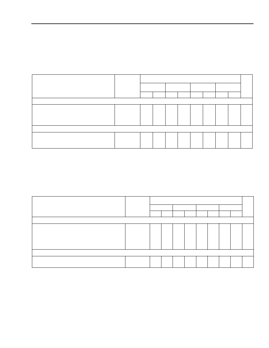
Table 46. PFU Output MUX and Direct Routing Timing Characteristics
OR3Cxx Commercial: VDD = 5.0 V ± 5%, 0 °C
< TA < 70 °C; Industrial: VDD = 5.0 V ± 10%, –40 °C < TA < +85 °C.
OR3Txxx Commercial: VDD = 3.0 V to 3.6 V, 0 °C
< TA < 70 °C; Industrial: VDD = 3.0 V to 3.6 V, –40 °C < TA < +85 °C.
* This is general feedback using switching segments. See the combinatorial PFU timing table for softwired look-up table feedback timing.
SLIC Timing
Table 47
. Supplemental Logic and Interconnect Cell (SLIC) Timing Characteristics
OR3Cxx Commercial: VDD = 5.0 V ± 5%, 0 °C
< TA < 70 °C; Industrial: VDD = 5.0 V ± 10%, –40 °C < TA < +85 °C.
OR3Txxx Commercial: VDD = 3.0 V to 3.6 V, 0 °C
< TA < 70 °C; Industrial: VDD = 3.0 V to 3.6 V, –40 °C < TA < +85 °C.
Parameter
(TJ = 85 °C, VDD = min)
Symbol
Speed
Unit
-4
-5
-6
-7
Min
Max
Min
Max
Min
Max
Min
Max
PFU Output MUX
(Fan-out = 1)
Output MUX Delay (F[7:0]/Q[7:0] to O[9:0])
Carry-out MUX Delay (COUT to O9)
Registered Carry-out MUX Delay (REGCOUT
to O8)
OMUX_DEL
COO9_DEL
RCOO8_DEL
—
0.50
0.34
—
0.39
0.26
—
0.35
0.24
—
0.28
0.18
ns
Direct Routing
PFU Feedback (xSW)*
PFU to Orthogonal PFU Delay (xSW to xSW)
PFU to Diagonal PFU Delay (xBID to xSW)
FDBK_DEL
ODIR_DEL
DDIR_DEL
—
1.74
2.21
2.69
—
1.41
1.77
2.19
—
1.48
1.75
2.53
—
1.14
1.39
1.98
ns
Parameter
(TJ = 85 °C, VDD = min)
Symbol
Speed
Unit
-4
-5
-6
-7
Min
Max
Min
Max
Min
Max
Min
Max
3-Statable BIDIs
BIDI Delay (BRx to BLx, BLx to BRx)
BIDI Delay (Ox to BRx, Ox to BLx)
BIDI 3-state Enable/Disable Delay (TRI to BL, BR)
BIDI 3-state Enable/Disable Delay
(BL, BR via DEC, TRI to BL, BR)
BUF_DEL
OBUF_DEL
TRI_DEL
DECTRI_DEL
—
0.84
0.72
2.55
3.59
—
0.70
0.61
1.90
2.65
—
0.94
0.87
1.31
1.91
—
0.77
0.70
1.01
1.48
ns
Decoder
Decoder Delay (BR[9:8], BL[9:8] to DEC)
Decoder Delay (BR[7:0], BL[7:0] to DEC)
DEC98_DEL
DEC_DEL
—
2.39
2.35
—
1.85
1.82
—
1.27
1.23
—
1.02
0.99
ns
Select
devices
have
been
discontinued.
See
Ordering
Information
section
for
product
status.
相關(guān)PDF資料 |
PDF描述 |
|---|---|
| OR3T556PS240-DB | FPGA, 324 CLBS, 80000 GATES, PQFP240 |
| OR3T806PS240-DB | FPGA, 484 CLBS, 116000 GATES, PQFP240 |
| OR3T807PS240-DB | FPGA, 484 CLBS, 116000 GATES, PQFP240 |
| OR3T55-4BA256I | FPGA, 324 CLBS, 40000 GATES, 80 MHz, PBGA256 |
| OR3T55-4BA256 | FPGA, 324 CLBS, 40000 GATES, 80 MHz, PBGA256 |
相關(guān)代理商/技術(shù)參數(shù) |
參數(shù)描述 |
|---|---|
| OR3T30-7S240I | 制造商:未知廠家 制造商全稱:未知廠家 功能描述:Field Programmable Gate Array (FPGA) |
| OR3T55 | 制造商:AGERE 制造商全稱:AGERE 功能描述:3C and 3T Field-Programmable Gate Arrays |
| OR3T55-4BA256I | 制造商:未知廠家 制造商全稱:未知廠家 功能描述:Field Programmable Gate Array (FPGA) |
| OR3T55-4PS208I | 制造商:未知廠家 制造商全稱:未知廠家 功能描述:Field Programmable Gate Array (FPGA) |
| OR3T55-4PS240I | 制造商:未知廠家 制造商全稱:未知廠家 功能描述:Field Programmable Gate Array (FPGA) |
發(fā)布緊急采購(gòu),3分鐘左右您將得到回復(fù)。