- 您現(xiàn)在的位置:買賣IC網(wǎng) > PDF目錄299575 > OR3T1257PS208-DB (LATTICE SEMICONDUCTOR CORP) FPGA, 784 CLBS, 186000 GATES, PQFP208 PDF資料下載
參數(shù)資料
| 型號(hào): | OR3T1257PS208-DB |
| 廠商: | LATTICE SEMICONDUCTOR CORP |
| 元件分類: | FPGA |
| 英文描述: | FPGA, 784 CLBS, 186000 GATES, PQFP208 |
| 封裝: | PLASTIC, SQFP2-208 |
| 文件頁(yè)數(shù): | 199/203頁(yè) |
| 文件大?。?/td> | 1368K |
| 代理商: | OR3T1257PS208-DB |
第1頁(yè)第2頁(yè)第3頁(yè)第4頁(yè)第5頁(yè)第6頁(yè)第7頁(yè)第8頁(yè)第9頁(yè)第10頁(yè)第11頁(yè)第12頁(yè)第13頁(yè)第14頁(yè)第15頁(yè)第16頁(yè)第17頁(yè)第18頁(yè)第19頁(yè)第20頁(yè)第21頁(yè)第22頁(yè)第23頁(yè)第24頁(yè)第25頁(yè)第26頁(yè)第27頁(yè)第28頁(yè)第29頁(yè)第30頁(yè)第31頁(yè)第32頁(yè)第33頁(yè)第34頁(yè)第35頁(yè)第36頁(yè)第37頁(yè)第38頁(yè)第39頁(yè)第40頁(yè)第41頁(yè)第42頁(yè)第43頁(yè)第44頁(yè)第45頁(yè)第46頁(yè)第47頁(yè)第48頁(yè)第49頁(yè)第50頁(yè)第51頁(yè)第52頁(yè)第53頁(yè)第54頁(yè)第55頁(yè)第56頁(yè)第57頁(yè)第58頁(yè)第59頁(yè)第60頁(yè)第61頁(yè)第62頁(yè)第63頁(yè)第64頁(yè)第65頁(yè)第66頁(yè)第67頁(yè)第68頁(yè)第69頁(yè)第70頁(yè)第71頁(yè)第72頁(yè)第73頁(yè)第74頁(yè)第75頁(yè)第76頁(yè)第77頁(yè)第78頁(yè)第79頁(yè)第80頁(yè)第81頁(yè)第82頁(yè)第83頁(yè)第84頁(yè)第85頁(yè)第86頁(yè)第87頁(yè)第88頁(yè)第89頁(yè)第90頁(yè)第91頁(yè)第92頁(yè)第93頁(yè)第94頁(yè)第95頁(yè)第96頁(yè)第97頁(yè)第98頁(yè)第99頁(yè)第100頁(yè)第101頁(yè)第102頁(yè)第103頁(yè)第104頁(yè)第105頁(yè)第106頁(yè)第107頁(yè)第108頁(yè)第109頁(yè)第110頁(yè)第111頁(yè)第112頁(yè)第113頁(yè)第114頁(yè)第115頁(yè)第116頁(yè)第117頁(yè)第118頁(yè)第119頁(yè)第120頁(yè)第121頁(yè)第122頁(yè)第123頁(yè)第124頁(yè)第125頁(yè)第126頁(yè)第127頁(yè)第128頁(yè)第129頁(yè)第130頁(yè)第131頁(yè)第132頁(yè)第133頁(yè)第134頁(yè)第135頁(yè)第136頁(yè)第137頁(yè)第138頁(yè)第139頁(yè)第140頁(yè)第141頁(yè)第142頁(yè)第143頁(yè)第144頁(yè)第145頁(yè)第146頁(yè)第147頁(yè)第148頁(yè)第149頁(yè)第150頁(yè)第151頁(yè)第152頁(yè)第153頁(yè)第154頁(yè)第155頁(yè)第156頁(yè)第157頁(yè)第158頁(yè)第159頁(yè)第160頁(yè)第161頁(yè)第162頁(yè)第163頁(yè)第164頁(yè)第165頁(yè)第166頁(yè)第167頁(yè)第168頁(yè)第169頁(yè)第170頁(yè)第171頁(yè)第172頁(yè)第173頁(yè)第174頁(yè)第175頁(yè)第176頁(yè)第177頁(yè)第178頁(yè)第179頁(yè)第180頁(yè)第181頁(yè)第182頁(yè)第183頁(yè)第184頁(yè)第185頁(yè)第186頁(yè)第187頁(yè)第188頁(yè)第189頁(yè)第190頁(yè)第191頁(yè)第192頁(yè)第193頁(yè)第194頁(yè)第195頁(yè)第196頁(yè)第197頁(yè)第198頁(yè)當(dāng)前第199頁(yè)第200頁(yè)第201頁(yè)第202頁(yè)第203頁(yè)
Lattice Semiconductor
95
Data Sheet
November 2006
ORCA Series 3C and 3T FPGAs
FPGA Conguration Modes (continued)
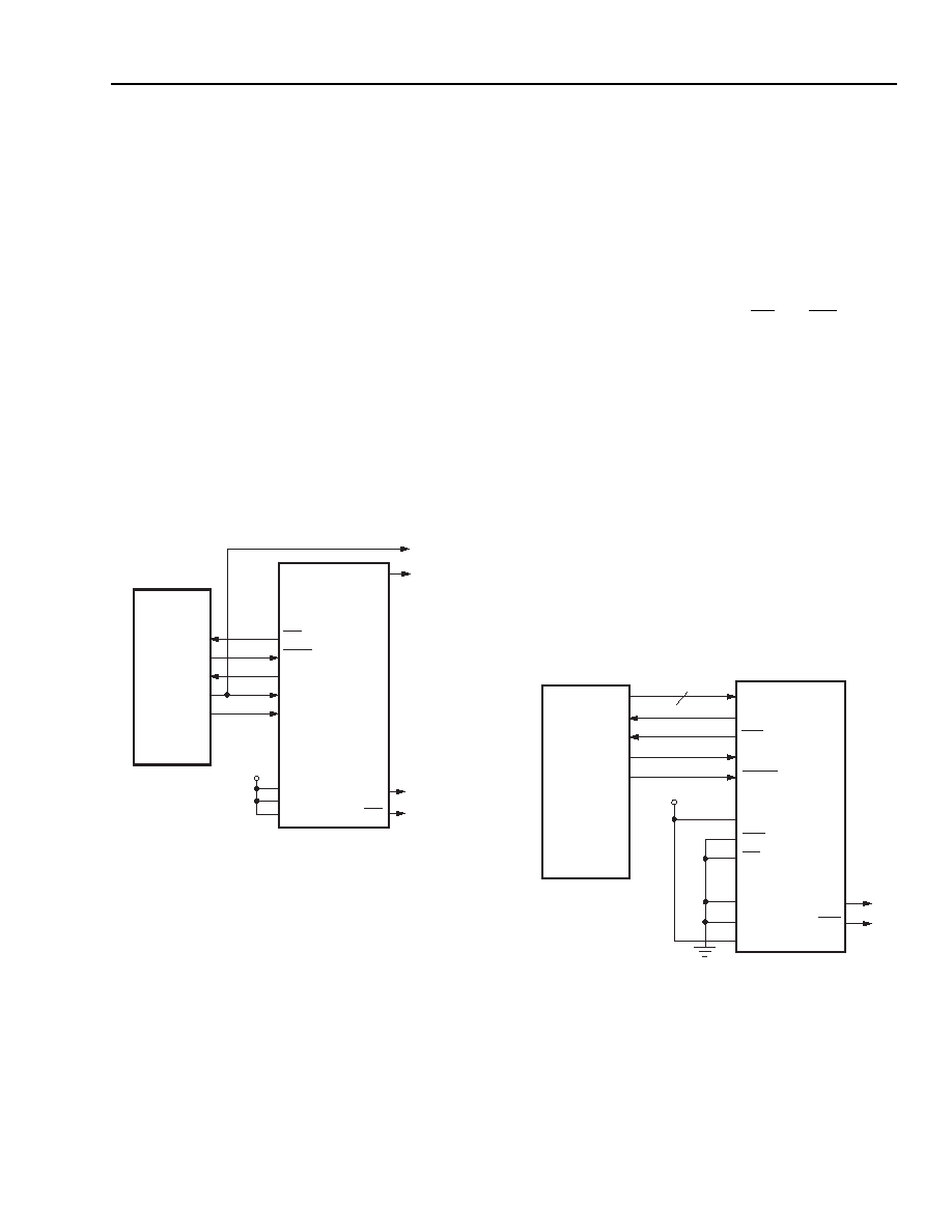
Slave Serial Mode
The slave serial mode is primarily used when multiple
FPGAs are congured in a daisy-chain (see the Daisy-
Chaining section). It is also used on the FPGA evalua-
tion board that interfaces to the download cable. A
device in the slave serial mode can be used as the lead
device in a daisy-chain. Figure 61 shows the connec-
tions for the slave serial conguration mode.
The conguration data is provided into the FPGA’s DIN
input synchronous with the conguration clock CCLK
input. After the FPGA has loaded its conguration data,
it retransmits the incoming conguration data on
DOUT. CCLK is routed into all slave serial mode
devices in parallel.
Multiple slave FPGAs can be loaded with identical con-
gurations simultaneously. This is done by loading the
conguration data into the DIN inputs in parallel.
5-4485(F)
Figure 61. Slave Serial Conguration Schematic
Slave Parallel Mode
The slave parallel mode is essentially the same as the
slave serial mode except that 8 bits of data are input on
pins D[7:0] for each CCLK cycle. Due to 8 bits of data
being input per CCLK cycle, the DOUT pin does not
contain a valid bit stream for slave parallel mode. As a
result, the lead device cannot be used in the slave
parallel mode in a daisy-chain conguration.
Figure 62 is a schematic of the connections for the
slave parallel conguration mode. WR and CS0 are
active-low chip select signals, and CS1 is an active-
high chip select signal. These chip selects allow the
user to congure multiple FPGAs in slave parallel
mode using an 8-bit data bus common to all of the
FPGAs. These chip selects can then be used to select
the FPGA(s) to be congured with a given bit stream.
The chip selects must be active for each valid CCLK
cycle until the device has been completely pro-
grammed. They can be inactive between cycles but
must meet the setup and hold times for each valid pos-
itive CCLK. D[7:0] of the FPGA can be connected to
D[7:0] of the microprocessor only if a standard prom
le format is used. If a .bit or .rbt le is used from
ispLEVER, then the user must mirror the bytes in the
.bit or .rbt le OR leave the .bit or .rbt le unchanged
and connect D[7:0] of the FPGA to D[0:7] of the micro-
processor.
5-4487(F)
Figure 62. Slave Parallel Conguration Schematic
MICRO-
PROCESSOR
OR
DOWNLOAD
CABLE
M2
M1
M0
HDC
SERIES
FPGA
LDC
VDD
CCLK
PRGM
DOUT
TO DAISY-
CHAINED
DEVICES
DONE
DIN
INIT
ORCA
MICRO-
PROCESSOR
OR
SYSTEM
D[7:0]
DONE
CCLK
CS1
M2
M1
M0
HDC
LDC
8
VDD
INIT
PRGM
CS0
WR
SERIES
FPGA
ORCA
Select
devices
have
been
discontinued.
See
Ordering
Information
section
for
product
status.
相關(guān)PDF資料 |
PDF描述 |
|---|---|
| OR3T306S240I-DB | FPGA, 196 CLBS, 48000 GATES, PQFP240 |
| OR3T307S240-DB | FPGA, 196 CLBS, 48000 GATES, PQFP240 |
| OR3T556PS240-DB | FPGA, 324 CLBS, 80000 GATES, PQFP240 |
| OR3T806PS240-DB | FPGA, 484 CLBS, 116000 GATES, PQFP240 |
| OR3T807PS240-DB | FPGA, 484 CLBS, 116000 GATES, PQFP240 |
相關(guān)代理商/技術(shù)參數(shù) |
參數(shù)描述 |
|---|---|
| OR3T125-7PS208I | 制造商:AGERE 制造商全稱:AGERE 功能描述:3C and 3T Field-Programmable Gate Arrays |
| OR3T125-7PS240 | 制造商:AGERE 制造商全稱:AGERE 功能描述:3C and 3T Field-Programmable Gate Arrays |
| OR3T1257PS240-DB | 功能描述:FPGA - 現(xiàn)場(chǎng)可編程門陣列 6272 LUT 342 I/O RoHS:否 制造商:Altera Corporation 系列:Cyclone V E 柵極數(shù)量: 邏輯塊數(shù)量:943 內(nèi)嵌式塊RAM - EBR:1956 kbit 輸入/輸出端數(shù)量:128 最大工作頻率:800 MHz 工作電源電壓:1.1 V 最大工作溫度:+ 70 C 安裝風(fēng)格:SMD/SMT 封裝 / 箱體:FBGA-256 |
| OR3T125-7PS240I | 制造商:AGERE 制造商全稱:AGERE 功能描述:3C and 3T Field-Programmable Gate Arrays |
| OR3T20 | 制造商:AGERE 制造商全稱:AGERE 功能描述:3C and 3T Field-Programmable Gate Arrays |
發(fā)布緊急采購(gòu),3分鐘左右您將得到回復(fù)。