- 您現(xiàn)在的位置:買賣IC網(wǎng) > PDF目錄299575 > OR3T1257PS208-DB (LATTICE SEMICONDUCTOR CORP) FPGA, 784 CLBS, 186000 GATES, PQFP208 PDF資料下載
參數(shù)資料
| 型號(hào): | OR3T1257PS208-DB |
| 廠商: | LATTICE SEMICONDUCTOR CORP |
| 元件分類: | FPGA |
| 英文描述: | FPGA, 784 CLBS, 186000 GATES, PQFP208 |
| 封裝: | PLASTIC, SQFP2-208 |
| 文件頁數(shù): | 176/203頁 |
| 文件大?。?/td> | 1368K |
| 代理商: | OR3T1257PS208-DB |
第1頁第2頁第3頁第4頁第5頁第6頁第7頁第8頁第9頁第10頁第11頁第12頁第13頁第14頁第15頁第16頁第17頁第18頁第19頁第20頁第21頁第22頁第23頁第24頁第25頁第26頁第27頁第28頁第29頁第30頁第31頁第32頁第33頁第34頁第35頁第36頁第37頁第38頁第39頁第40頁第41頁第42頁第43頁第44頁第45頁第46頁第47頁第48頁第49頁第50頁第51頁第52頁第53頁第54頁第55頁第56頁第57頁第58頁第59頁第60頁第61頁第62頁第63頁第64頁第65頁第66頁第67頁第68頁第69頁第70頁第71頁第72頁第73頁第74頁第75頁第76頁第77頁第78頁第79頁第80頁第81頁第82頁第83頁第84頁第85頁第86頁第87頁第88頁第89頁第90頁第91頁第92頁第93頁第94頁第95頁第96頁第97頁第98頁第99頁第100頁第101頁第102頁第103頁第104頁第105頁第106頁第107頁第108頁第109頁第110頁第111頁第112頁第113頁第114頁第115頁第116頁第117頁第118頁第119頁第120頁第121頁第122頁第123頁第124頁第125頁第126頁第127頁第128頁第129頁第130頁第131頁第132頁第133頁第134頁第135頁第136頁第137頁第138頁第139頁第140頁第141頁第142頁第143頁第144頁第145頁第146頁第147頁第148頁第149頁第150頁第151頁第152頁第153頁第154頁第155頁第156頁第157頁第158頁第159頁第160頁第161頁第162頁第163頁第164頁第165頁第166頁第167頁第168頁第169頁第170頁第171頁第172頁第173頁第174頁第175頁當(dāng)前第176頁第177頁第178頁第179頁第180頁第181頁第182頁第183頁第184頁第185頁第186頁第187頁第188頁第189頁第190頁第191頁第192頁第193頁第194頁第195頁第196頁第197頁第198頁第199頁第200頁第201頁第202頁第203頁
74
Lattice Semiconductor
Data Sheet
November 2006
ORCA Series 3C and 3T FPGAs
Programmable Clock Manager (PCM)
(continued)
2x Clock Duty-Cycle Adjustment
A doubled-frequency, duty-cycle adjusted version of
the input clock can be constructed in DLL mode. The
rst clock cycle of the 2x clock output occurs when the
input clock is high, and the second cycle occurs when
the input clock is low. The duty cycle can be adjusted in
1/32 (6.25%) increments of the input clock period.
Additionally, each of the two doubled-clock cycles that
occurs in a single input clock cycle may be adjusted to
have different duty cycles. DLL 2x clock mode is
selected by setting bit 4 of register ve to a 1, and by
setting register six, bits [5:4] to 01 for ExpressCLK out-
put, and/or bits [7:6] to 01 for system clock output. The
duty-cycle percentage value is entered in register
three. See register three programming details for more
information. Duty-cycle values where both cycles of the
doubled clock have the same duty cycle are also
shown in Table 28.
Table 28. DLL Mode Delay/2x Duty Cycle
Programming Values
Phase-Locked Loop (PLL) Mode
The PLL mode of the PCM is used for clock multiplica-
tion (1/8x to 64x) and clock delay minimization func-
tions. PLL functions make use of the PCM dividers and
use feedback signals, often from the FPGA array. The
use of feedback is discussed with each PLL submode.
PLL mode is selected by setting bit 0 of register ve to
1.
Clock Delay Minimization
PLL mode can be used to minimize the effects of the
input buffer and input routing delay on the clock signal.
PLL mode causes a feedback clock signal to align in
phase with the input clock (refer back to the block dia-
gram in Figure 45) so that the delay between them is
effectively eliminated.
There is a dedicated feedback path from an adjacent
middle CLKCNTRL block to the PCM. Using the corner
ExpressCLK
pad as the input to the PCM and using this
dedicated feedback path, the clock from the Express-
CLK
output of the PCM, as viewed at the CLKCNTRL
block, will be phase-aligned with the ExpressCLK input
to the PCM. These relationships are diagrammed in
Figure 47.
A feedback clock can also be input to the PCM from
general routing. This allows for compensating for delay
between the PCM input and a point in the general rout-
ing. The use of this routed-feedback path is not gener-
ally recommended. Because compensation is based
on the programmable routing, the amount of clock
delay compensation can vary between FPGA lots and
fabrication processes, and will vary each time that the
feedback line is routed using different resources. Con-
tact Lattice for application notes regarding the use of
routed-feedback delay compensation.
5-5980(F)
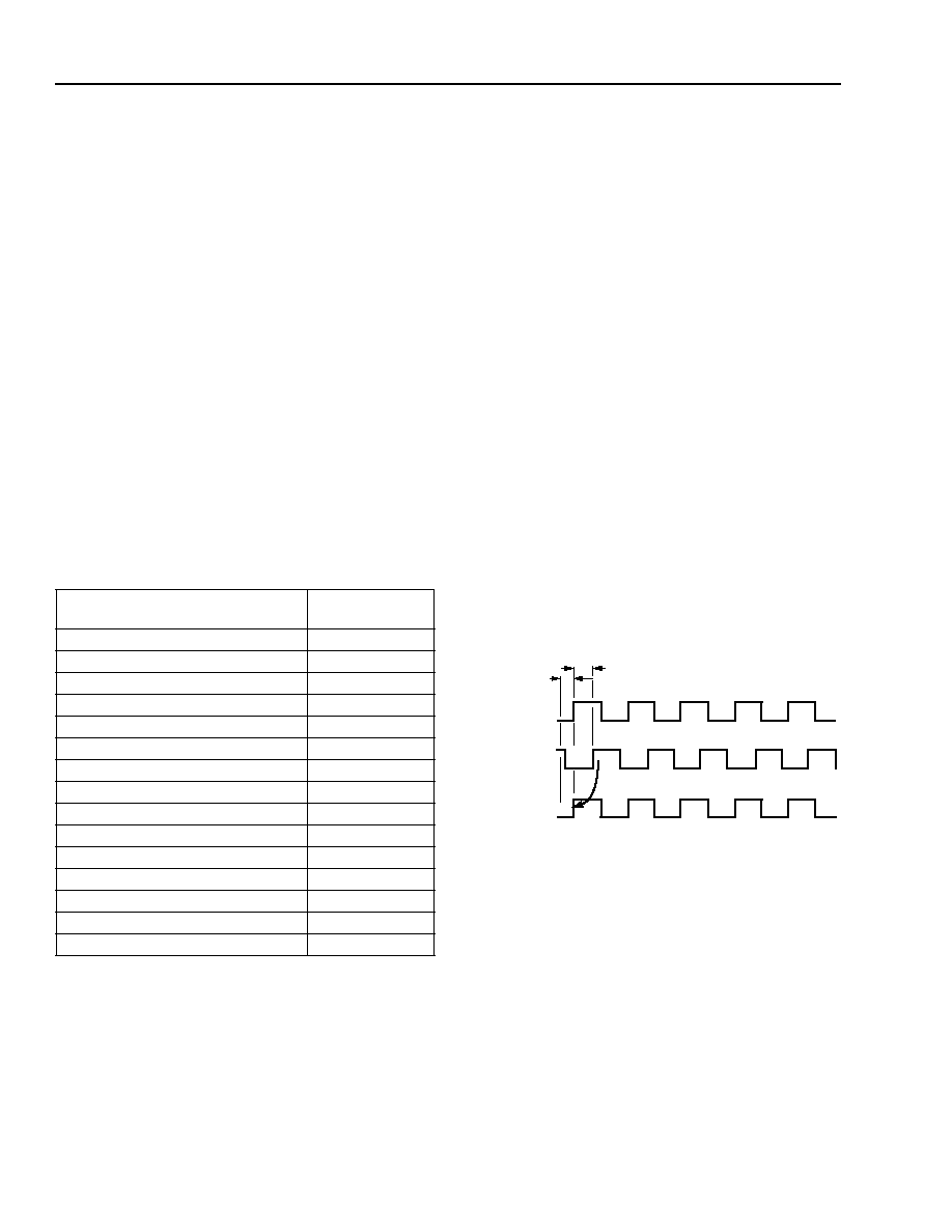
Figure 47. ExpressCLK Delay Minimization
Using the PCM
Register 3 [7:0]
7 6 5 4 3 2 1 0
Duty Cycle
(%)
0 0 0 0 0 0 0 0
6.25
0 0 0 0 1 0 0 1
12.50
0 0 0 1 0 0 1 0
18.75
0 0 0 1 1 0 1 1
25.00
0 0 1 0 0 1 0 0
31.25
0 0 1 0 1 1 0 1
37.50
0 0 1 1 0 1 1 0
43.75
0 0 1 1 1 1 1 1
50.00
1 1 0 0 0 0 0 0
56.25
1 1 0 0 1 0 0 1
62.50
1 1 0 1 0 0 1 0
68.75
1 1 0 1 1 0 1 1
75.00
1 1 1 0 0 1 0 0
81.25
1 1 1 0 1 1 0 1
87.50
1 1 1 1 0 1 1 0
93.75
CORNER
CLKCNTRL
DELAY
DELAY IS COMPENSATED
INPUT
OUTPUT WITHOUT
USING PCM
OUTPUT
EXPRESSCLK
USING PCM
EXPRESSCLK
COMPENSATION EQUALS DELAY
Select
devices
have
been
discontinued.
See
Ordering
Information
section
for
product
status.
相關(guān)PDF資料 |
PDF描述 |
|---|---|
| OR3T306S240I-DB | FPGA, 196 CLBS, 48000 GATES, PQFP240 |
| OR3T307S240-DB | FPGA, 196 CLBS, 48000 GATES, PQFP240 |
| OR3T556PS240-DB | FPGA, 324 CLBS, 80000 GATES, PQFP240 |
| OR3T806PS240-DB | FPGA, 484 CLBS, 116000 GATES, PQFP240 |
| OR3T807PS240-DB | FPGA, 484 CLBS, 116000 GATES, PQFP240 |
相關(guān)代理商/技術(shù)參數(shù) |
參數(shù)描述 |
|---|---|
| OR3T125-7PS208I | 制造商:AGERE 制造商全稱:AGERE 功能描述:3C and 3T Field-Programmable Gate Arrays |
| OR3T125-7PS240 | 制造商:AGERE 制造商全稱:AGERE 功能描述:3C and 3T Field-Programmable Gate Arrays |
| OR3T1257PS240-DB | 功能描述:FPGA - 現(xiàn)場(chǎng)可編程門陣列 6272 LUT 342 I/O RoHS:否 制造商:Altera Corporation 系列:Cyclone V E 柵極數(shù)量: 邏輯塊數(shù)量:943 內(nèi)嵌式塊RAM - EBR:1956 kbit 輸入/輸出端數(shù)量:128 最大工作頻率:800 MHz 工作電源電壓:1.1 V 最大工作溫度:+ 70 C 安裝風(fēng)格:SMD/SMT 封裝 / 箱體:FBGA-256 |
| OR3T125-7PS240I | 制造商:AGERE 制造商全稱:AGERE 功能描述:3C and 3T Field-Programmable Gate Arrays |
| OR3T20 | 制造商:AGERE 制造商全稱:AGERE 功能描述:3C and 3T Field-Programmable Gate Arrays |
發(fā)布緊急采購,3分鐘左右您將得到回復(fù)。