- 您現(xiàn)在的位置:買賣IC網(wǎng) > PDF目錄299575 > OR3T1256PS240I-DB (LATTICE SEMICONDUCTOR CORP) FPGA, 784 CLBS, 186000 GATES, PQFP240 PDF資料下載
參數(shù)資料
| 型號: | OR3T1256PS240I-DB |
| 廠商: | LATTICE SEMICONDUCTOR CORP |
| 元件分類: | FPGA |
| 英文描述: | FPGA, 784 CLBS, 186000 GATES, PQFP240 |
| 封裝: | PLASTIC, SQFP2-240 |
| 文件頁數(shù): | 154/203頁 |
| 文件大小: | 1368K |
| 代理商: | OR3T1256PS240I-DB |
第1頁第2頁第3頁第4頁第5頁第6頁第7頁第8頁第9頁第10頁第11頁第12頁第13頁第14頁第15頁第16頁第17頁第18頁第19頁第20頁第21頁第22頁第23頁第24頁第25頁第26頁第27頁第28頁第29頁第30頁第31頁第32頁第33頁第34頁第35頁第36頁第37頁第38頁第39頁第40頁第41頁第42頁第43頁第44頁第45頁第46頁第47頁第48頁第49頁第50頁第51頁第52頁第53頁第54頁第55頁第56頁第57頁第58頁第59頁第60頁第61頁第62頁第63頁第64頁第65頁第66頁第67頁第68頁第69頁第70頁第71頁第72頁第73頁第74頁第75頁第76頁第77頁第78頁第79頁第80頁第81頁第82頁第83頁第84頁第85頁第86頁第87頁第88頁第89頁第90頁第91頁第92頁第93頁第94頁第95頁第96頁第97頁第98頁第99頁第100頁第101頁第102頁第103頁第104頁第105頁第106頁第107頁第108頁第109頁第110頁第111頁第112頁第113頁第114頁第115頁第116頁第117頁第118頁第119頁第120頁第121頁第122頁第123頁第124頁第125頁第126頁第127頁第128頁第129頁第130頁第131頁第132頁第133頁第134頁第135頁第136頁第137頁第138頁第139頁第140頁第141頁第142頁第143頁第144頁第145頁第146頁第147頁第148頁第149頁第150頁第151頁第152頁第153頁當(dāng)前第154頁第155頁第156頁第157頁第158頁第159頁第160頁第161頁第162頁第163頁第164頁第165頁第166頁第167頁第168頁第169頁第170頁第171頁第172頁第173頁第174頁第175頁第176頁第177頁第178頁第179頁第180頁第181頁第182頁第183頁第184頁第185頁第186頁第187頁第188頁第189頁第190頁第191頁第192頁第193頁第194頁第195頁第196頁第197頁第198頁第199頁第200頁第201頁第202頁第203頁
54
Lattice Semiconductor
Data Sheet
November 2006
ORCA Series 3C and 3T FPGAs
Special Function Blocks (continued)
Start-Up Logic
The start-up logic block is located in the lower right cor-
ner of the FPGA. This block can be congured to coor-
dinate the relative timing of the release of GSRN, the
activation of all user I/Os, and the assertion of the
DONE signal at the end of conguration. If a start-up
clock is used to time these events, the start-up clock
can come from CCLK, or it can be routed into the start-
up block using lower right corner routing resources.
These signals are described in the Start-Up subsection
of the FPGA States of Operation section.
Clock Control (CLKCNTRL) and StopCLK
There is one CLKCNTRL block in the MID section of
the interquad routing on each side of the FPGA. This
block is used to selectively distribute the fast clock to
the PLC array and the left (top) and right (bottom)
ExpressCLKs (ECKL and ECKR) to the side of the
array on which the CLKCNTRL block resides.
The source clock for the CLKCNTRL block comes
either from the ExpressCLK pad at the middle of the
side of the FPGA or from the corner ExpressCLK route
that comes from the corner ExpressCLK pad (at the
lower left or upper right of the device, whichever is
closer). The programmable clock manager ExpressCLK
output can also be sourced to this corner routing for
distribution at the two closest CLKCNTRL blocks.
Each CLKCNTRL block also features an invertible
StopCLK
shutoff input that is available from local rout-
ing. This feature may be used to glitchlessly stop and
start the clock at the three outputs of each CLKCNTRL
block and has the option of doing so on either the rising
or falling edge of the clock. When the clock is halted
based on its rising edge, it stops and stays at VDD.
When it is stopped based on its falling edge, it stops
and stays at GND. If the StopCLK shutoff signal meets
the CLKCNTRL setup and hold times, the clock is
stopped on the second clock cycle after the shutoff sig-
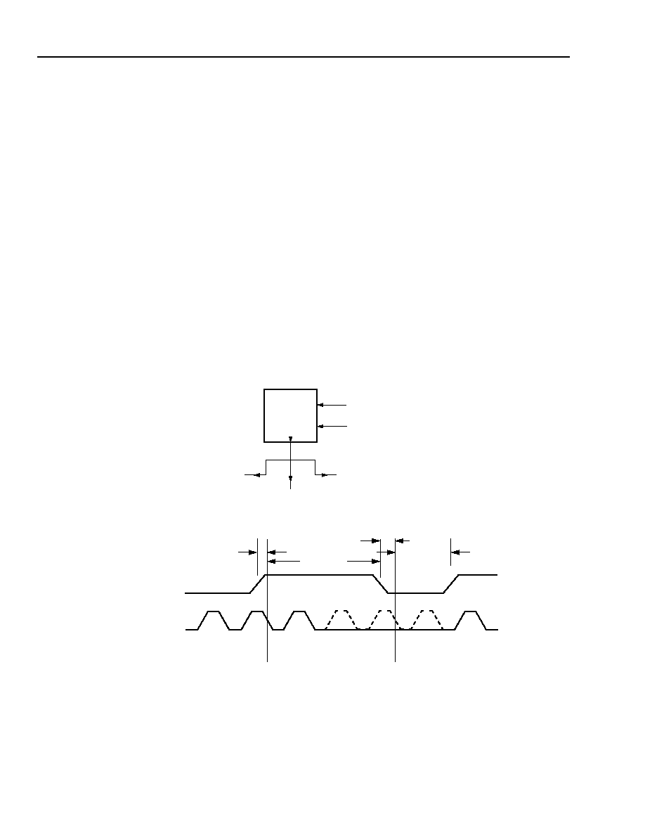
nal. A diagram of the bottom CLKCNTRL block and
StopCLK
timing is shown in Figure 35.
5-5981(F)
Notes:
CLKCNTRL output clocks are ExpressCLK left and right and fast clock.
Clock shutoff shown active-high acting on clock falling edge.
Figure 35. Top CLKCNTRL Function Block
CORNER EXPRESSCLK
CLOCK SHUTOFF
EXPRESSCLK RIGHT
EXPRESSCLK LEFT
FAST CLOCK
CLOCK SHUTOFF
OFF_SET
OFF_HLD
OFF_SET
OFF_HLD
CLKCNTRL OUTPUT
CLOCKS
Select
devices
have
been
discontinued.
See
Ordering
Information
section
for
product
status.
相關(guān)PDF資料 |
PDF描述 |
|---|---|
| OR3T1257PS208-DB | FPGA, 784 CLBS, 186000 GATES, PQFP208 |
| OR3T306S240I-DB | FPGA, 196 CLBS, 48000 GATES, PQFP240 |
| OR3T307S240-DB | FPGA, 196 CLBS, 48000 GATES, PQFP240 |
| OR3T556PS240-DB | FPGA, 324 CLBS, 80000 GATES, PQFP240 |
| OR3T806PS240-DB | FPGA, 484 CLBS, 116000 GATES, PQFP240 |
相關(guān)代理商/技術(shù)參數(shù) |
參數(shù)描述 |
|---|---|
| OR3T125-7BA352 | 制造商:AGERE 制造商全稱:AGERE 功能描述:3C and 3T Field-Programmable Gate Arrays |
| OR3T1257BA352-DB | 功能描述:FPGA - 現(xiàn)場可編程門陣列 6272 LUT 342 I/O RoHS:否 制造商:Altera Corporation 系列:Cyclone V E 柵極數(shù)量: 邏輯塊數(shù)量:943 內(nèi)嵌式塊RAM - EBR:1956 kbit 輸入/輸出端數(shù)量:128 最大工作頻率:800 MHz 工作電源電壓:1.1 V 最大工作溫度:+ 70 C 安裝風(fēng)格:SMD/SMT 封裝 / 箱體:FBGA-256 |
| OR3T125-7BA352I | 制造商:AGERE 制造商全稱:AGERE 功能描述:3C and 3T Field-Programmable Gate Arrays |
| OR3T125-7BC432 | 制造商:AGERE 制造商全稱:AGERE 功能描述:3C and 3T Field-Programmable Gate Arrays |
| OR3T1257BC432-DB | 功能描述:FPGA - 現(xiàn)場可編程門陣列 6272 LUT 342 I/O RoHS:否 制造商:Altera Corporation 系列:Cyclone V E 柵極數(shù)量: 邏輯塊數(shù)量:943 內(nèi)嵌式塊RAM - EBR:1956 kbit 輸入/輸出端數(shù)量:128 最大工作頻率:800 MHz 工作電源電壓:1.1 V 最大工作溫度:+ 70 C 安裝風(fēng)格:SMD/SMT 封裝 / 箱體:FBGA-256 |
發(fā)布緊急采購,3分鐘左右您將得到回復(fù)。