- 您現(xiàn)在的位置:買賣IC網(wǎng) > PDF目錄299576 > OR3T125-4B432 FPGA, 784 CLBS, 92000 GATES, PBGA432 PDF資料下載
參數(shù)資料
| 型號(hào): | OR3T125-4B432 |
| 元件分類: | FPGA |
| 英文描述: | FPGA, 784 CLBS, 92000 GATES, PBGA432 |
| 封裝: | BGA-432 |
| 文件頁(yè)數(shù): | 5/210頁(yè) |
| 文件大小: | 2138K |
| 代理商: | OR3T125-4B432 |
第1頁(yè)第2頁(yè)第3頁(yè)第4頁(yè)當(dāng)前第5頁(yè)第6頁(yè)第7頁(yè)第8頁(yè)第9頁(yè)第10頁(yè)第11頁(yè)第12頁(yè)第13頁(yè)第14頁(yè)第15頁(yè)第16頁(yè)第17頁(yè)第18頁(yè)第19頁(yè)第20頁(yè)第21頁(yè)第22頁(yè)第23頁(yè)第24頁(yè)第25頁(yè)第26頁(yè)第27頁(yè)第28頁(yè)第29頁(yè)第30頁(yè)第31頁(yè)第32頁(yè)第33頁(yè)第34頁(yè)第35頁(yè)第36頁(yè)第37頁(yè)第38頁(yè)第39頁(yè)第40頁(yè)第41頁(yè)第42頁(yè)第43頁(yè)第44頁(yè)第45頁(yè)第46頁(yè)第47頁(yè)第48頁(yè)第49頁(yè)第50頁(yè)第51頁(yè)第52頁(yè)第53頁(yè)第54頁(yè)第55頁(yè)第56頁(yè)第57頁(yè)第58頁(yè)第59頁(yè)第60頁(yè)第61頁(yè)第62頁(yè)第63頁(yè)第64頁(yè)第65頁(yè)第66頁(yè)第67頁(yè)第68頁(yè)第69頁(yè)第70頁(yè)第71頁(yè)第72頁(yè)第73頁(yè)第74頁(yè)第75頁(yè)第76頁(yè)第77頁(yè)第78頁(yè)第79頁(yè)第80頁(yè)第81頁(yè)第82頁(yè)第83頁(yè)第84頁(yè)第85頁(yè)第86頁(yè)第87頁(yè)第88頁(yè)第89頁(yè)第90頁(yè)第91頁(yè)第92頁(yè)第93頁(yè)第94頁(yè)第95頁(yè)第96頁(yè)第97頁(yè)第98頁(yè)第99頁(yè)第100頁(yè)第101頁(yè)第102頁(yè)第103頁(yè)第104頁(yè)第105頁(yè)第106頁(yè)第107頁(yè)第108頁(yè)第109頁(yè)第110頁(yè)第111頁(yè)第112頁(yè)第113頁(yè)第114頁(yè)第115頁(yè)第116頁(yè)第117頁(yè)第118頁(yè)第119頁(yè)第120頁(yè)第121頁(yè)第122頁(yè)第123頁(yè)第124頁(yè)第125頁(yè)第126頁(yè)第127頁(yè)第128頁(yè)第129頁(yè)第130頁(yè)第131頁(yè)第132頁(yè)第133頁(yè)第134頁(yè)第135頁(yè)第136頁(yè)第137頁(yè)第138頁(yè)第139頁(yè)第140頁(yè)第141頁(yè)第142頁(yè)第143頁(yè)第144頁(yè)第145頁(yè)第146頁(yè)第147頁(yè)第148頁(yè)第149頁(yè)第150頁(yè)第151頁(yè)第152頁(yè)第153頁(yè)第154頁(yè)第155頁(yè)第156頁(yè)第157頁(yè)第158頁(yè)第159頁(yè)第160頁(yè)第161頁(yè)第162頁(yè)第163頁(yè)第164頁(yè)第165頁(yè)第166頁(yè)第167頁(yè)第168頁(yè)第169頁(yè)第170頁(yè)第171頁(yè)第172頁(yè)第173頁(yè)第174頁(yè)第175頁(yè)第176頁(yè)第177頁(yè)第178頁(yè)第179頁(yè)第180頁(yè)第181頁(yè)第182頁(yè)第183頁(yè)第184頁(yè)第185頁(yè)第186頁(yè)第187頁(yè)第188頁(yè)第189頁(yè)第190頁(yè)第191頁(yè)第192頁(yè)第193頁(yè)第194頁(yè)第195頁(yè)第196頁(yè)第197頁(yè)第198頁(yè)第199頁(yè)第200頁(yè)第201頁(yè)第202頁(yè)第203頁(yè)第204頁(yè)第205頁(yè)第206頁(yè)第207頁(yè)第208頁(yè)第209頁(yè)第210頁(yè)
Preliminary Data Sheet, Rev. 1
ORCA Series 3 FPGAs
September 1998
102
Lucent Technologies Inc.
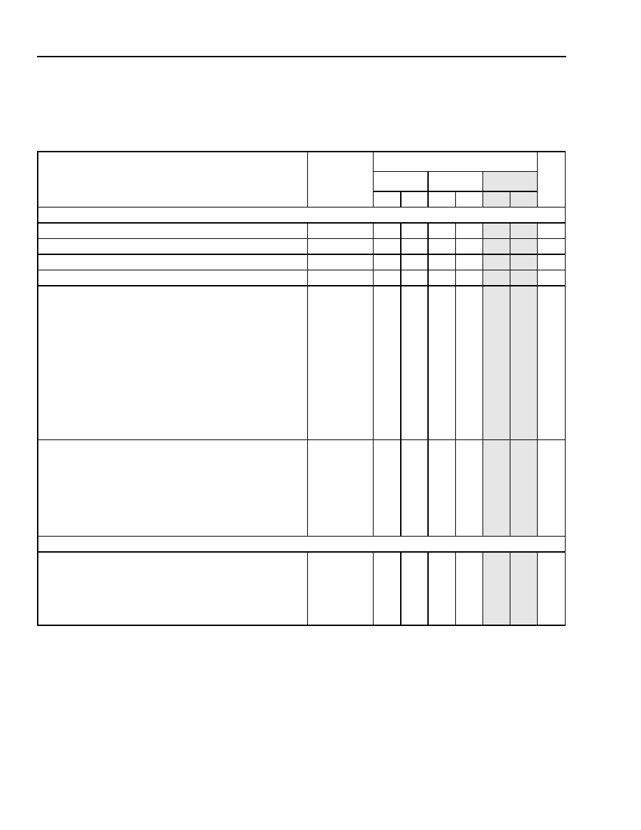
Timing Characteristics (continued)
Table 41. Sequential PFU Timing Characteristics
OR3Cxx Commercial: VDD = 5.0 V ± 5%, 0 °C
< TA < 70 °C; Industrial: VDD = 5.0 V ± 10%, –40 °C < TA < +85 °C.
OR3Txxx Commercial: VDD = 3.0 V to 3.6 V, 0 °C
< TA < 70 °C; Industrial: VDD = 3.0 V to 3.6 V, –40 °C < TA < +85 °C.
Parameter
Symbol
Speed
Unit
-4
-5
-6
Min
Max
Min
Max
Min
Max
Input Requirements
Clock Low Time
CLKL_MPW
3.36
—
2.07
—
1.16
—ns
Clock High Time
CLKH_MPW
1.61
—
1.06
—
0.70
—ns
Global S/R Pulse Width (GSRN)
GSR_MPW
3.36
—
2.07
—
1.16
—ns
Local S/R Pulse Width
LSR_MPW
3.36
—
2.07
—
1.16
—ns
Combinatorial Setup Times (TJ = +85 °C, VDD = min):
Four-input Variables to Clock (Kz[3:0] to CLK)*
Five-input Variables to Clock (F5[A:D] to CLK)
Data In to Clock (DIN[7:0] to CLK)
Carry-in to Clock, DIRECT to REGCOUT (CIN to CLK)
Clock Enable to Clock (CE to CLK)
Clock Enable to Clock (ASWE to CLK)
Local Set/Reset to Clock (SYNC) (LSR to CLK)
Data Select to Clock (SEL to CLK)
Two-level LUT to Clock (Kz[3:0] to CLK w/feedbk)*
Two-level LUT to Clock (F5[A:D] to CLK w/feedbk)
Three-level LUT to Clock (Kz[3:0] to CLK w/feedbk)*
Three-level LUT to Clock (F5[A:D] to CLK w/feedbk)
F4_SET
F5_SET
DIN_SET
CINDIR_SET
CE1_SET
CE2_SET
LSR_SET
SEL_SET
SWL2_SET
SWL2F5_SET
SWL3_SET
SWL3F5_SET
1.99
1.79
0.47
1.25
3.04
1.91
9.67
1.37
4.56
4.38
6.55
6.53
—
1.47
1.33
0.32
0.99
2.23
1.43
6.51
1.00
3.32
3.18
4.85
4.81
—
1.12
0.93
0.28
0.78
1.61
1.06
4.20
0.71
2.44
2.25
3.44
3.32
—
ns
Combinatorial Hold Times (TJ = all, VDD = all):
Data In (DIN[7:0] from CLK)
Carry-in from Clock, DIRECT to REGCOUT (CIN from CLK)
Clock Enable (CE from CLK)
Clock Enable from Clock (ASWE from CLK)
Local Set/Reset from Clock (sync) (LSR from CLK)
Data Select from Clock (SEL from CLK)
All Others
DIN_HLD
CINDIR_HLD
CE1_HLD
CE2_HLD
LSR_HLD
SEL_HLD
—
0.00
—
0.00
—
0.00
—
ns
Output Characteristics
Sequential Delays (TJ = +85 °C, VDD = min):
Local S/R (async) to PFU Out (LSR to Q[7:0], REGCOUT)
Global S/R to PFU Out (GSRN to Q[7:0], REGCOUT)
Clock to PFU Out—Register (CLK to Q[7:0], REGCOUT)
Clock to PFU Out—Latch (CLK to Q[7:0])
Transparent Latch (DIN[7:0] to Q[7:0])
LSR_DEL
GSR_DEL
REG_DEL
LTCH_DEL
LTCHD_DEL
—
7.02
5.21
2.38
2.51
2.73
—
5.29
3.90
1.75
1.88
2.10
—
3.79
2.76
1.26
1.33
1.56
ns
* Four-input variables’ (KZ[3:0]) setup times are valid for LUTs in both F4 (four-input LUT) and F5 (five-input LUT) modes.
ORCA Foundry may, in rare routing instances, report a slightly larger value for this parameter; in which case, ORCA Foundry results take
precedence.
Notes:
Shaded values are advance information and are valid for OR3Txxx devices only.
The table shows worst-case delays. ORCA Foundry reports the delays for individual paths within a group of paths representing the same
timing parameter and may accurately report delays that are less than those listed.
相關(guān)PDF資料 |
PDF描述 |
|---|---|
| OR3T125-4B600 | FPGA, 784 CLBS, 92000 GATES, PBGA600 |
| OR3T125-4BA352I | FPGA, 784 CLBS, 92000 GATES, PBGA352 |
| OR3T125-4BA352 | FPGA, 784 CLBS, 92000 GATES, PBGA352 |
| OR3T125-5B432 | FPGA, 784 CLBS, 92000 GATES, PBGA432 |
| OR3T125-5B600 | FPGA, 784 CLBS, 92000 GATES, PBGA600 |
相關(guān)代理商/技術(shù)參數(shù) |
參數(shù)描述 |
|---|---|
| OR3T125-4BC432I | 制造商:未知廠家 制造商全稱:未知廠家 功能描述:Field Programmable Gate Array (FPGA) |
| OR3T125-4BC600I | 制造商:未知廠家 制造商全稱:未知廠家 功能描述:Field Programmable Gate Array (FPGA) |
| OR3T125-4PS208I | 制造商:未知廠家 制造商全稱:未知廠家 功能描述:Field Programmable Gate Array (FPGA) |
| OR3T125-4PS240I | 制造商:未知廠家 制造商全稱:未知廠家 功能描述:Field Programmable Gate Array (FPGA) |
| OR3T125-5BA352 | 制造商:AGERE 制造商全稱:AGERE 功能描述:3C and 3T Field-Programmable Gate Arrays |
發(fā)布緊急采購(gòu),3分鐘左右您將得到回復(fù)。