- 您現(xiàn)在的位置:買(mǎi)賣(mài)IC網(wǎng) > PDF目錄382355 > MX803A (Electronic Theatre Controls, Inc.) Audio Signaling Processor PDF資料下載
參數(shù)資料
| 型號(hào): | MX803A |
| 廠商: | Electronic Theatre Controls, Inc. |
| 英文描述: | Audio Signaling Processor |
| 中文描述: | 音頻信號(hào)處理器 |
| 文件頁(yè)數(shù): | 4/26頁(yè) |
| 文件大?。?/td> | 225K |
| 代理商: | MX803A |
第1頁(yè)第2頁(yè)第3頁(yè)當(dāng)前第4頁(yè)第5頁(yè)第6頁(yè)第7頁(yè)第8頁(yè)第9頁(yè)第10頁(yè)第11頁(yè)第12頁(yè)第13頁(yè)第14頁(yè)第15頁(yè)第16頁(yè)第17頁(yè)第18頁(yè)第19頁(yè)第20頁(yè)第21頁(yè)第22頁(yè)第23頁(yè)第24頁(yè)第25頁(yè)第26頁(yè)

Audio Signaling Processor
4
MX803A PRELIMINARY INFORMATION
1996 MX
COM, INC.
Tele: 800 638 5577 910 744 5050 Fax: 910 744 5054
Doc. # 20480122.003
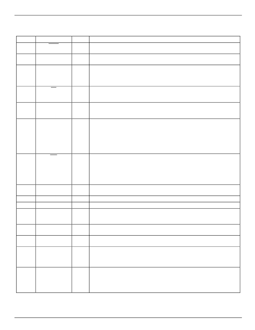
2. Signal List
Pin No.
1
Name
XTAL
Type
Output
Description
Output of the on-chip clock oscillator. External components are required at this
output when a Xtal is used. See Figure 2.
Input to the on-chip clock oscillator inverter. A Xtal or externally derived clock
should be connected here. See Figure 2.
C-BUS serial data output to the
μ
C. The transmission of Reply Data bytes is
synchronized to the Serial Clock under the control of the Chip Select input.
This 3-state output is held at high impedance when not sending data to the
μ
C.
See Figure 8 and Figure 9.
C-BUS data loading control function. This input is provided by the
μ
C. Data
transfer sequences are initiated, completed or aborted by the chip select signal.
See Figure 8 and Figure 9.
C-BUS serial data input from the
μ
C. Data is loaded to this device in 8-bit
bytes, MSB (B7) first and LSB (B0) last, synchronized to the Serial Clock. See
Figure 8 and Figure 9.
This “real-time” input is available as a general purpose logic input port which
can be read from the Status Register. See Table 3.
G/Purpose Timer Period Expired
NOTONE Timer Period Expired
RX Tone Measurement Complete
These interrupts are inactive during relevant powersave conditions and can be
disabled by bits 5 and 6 in the Control Register.
Output of this pin indicates an interrupt condition to the
μ
C by going to a logic
“0.” This is a “wire-or-able” output, allowing the connection of up to 8
peripherals to 1 interrupt port on the
μ
C. This pin has a low impedance
pulldown to logic “0” when active and a high impedance when inactive. The
system IRQ line requires one pullup resistor to V
DD
. The conditions that cause
interrupts are indicated in the Status Register and are shown below:
Input to the stand-alone on-chip Audio Switch. This function is
enabled/disabled by Bit 7 of the Control Register
Output of the stand-alone on-chip Audio Switch..
Negative supply (GND).
Received audio tone signaling input. This input must be ac coupled and
connected, using external components, to the Signal Input Bias pin. See Figure
2.
External components are required between this input and the RX Audio In pin.
See Figure 2.
Internal circuitry bias signal, held at V
DD
/2. This pin should be decoupled to V
SS
by capacitor C2. See Figure 2..
Tone 1 Generator (2-/5-tone Selcall or DTMF 1) output. External gain and
coupling components are required at this output when operating in a complete
DBS 800 audio installation. The frequency of this output is determined by
writing to the TX Tone Generator 1 Register (Table 5). See Figure 2.
Tone 2 Generator (2-/5-tone Selcall, CUES or DTMF 2) output. External gain
and coupling components are required at this output when operating in a
complete DBS 800 audio installation. The frequency of this output is
determined by writing to the TX Tone Generator 2 Register (Table 5).
See Figure 2.
2
Xtal/Clock
Input
3
Reply Data
Output
4
CS
Input
5
Command Data
Input
6
Logic Input
Input
7
IRQ
Output
10
Audio Switch In
Input
11
12
13
Audio Switch Out
V
SS
Rx Audio In
Output
Power
Input
14
Signal Input Bias
Input
15
V
BIAS
Output
16
Tone 1 Out
Output
17
Tone 2 Out
Output
相關(guān)PDF資料 |
PDF描述 |
|---|---|
| MX812 | VSR CODEC WITH DRAM CONTROL |
| MX812DW | VSR CODEC WITH DRAM CONTROL |
| MX812J | VSR CODEC WITH DRAM CONTROL |
| MX841 | White LED Step-Up Converter |
| MX88L284AEC | Highly integration chip for Flat Panel Display application |
相關(guān)代理商/技術(shù)參數(shù) |
參數(shù)描述 |
|---|---|
| MX803ADW | 制造商:CML Innovative Technologies 功能描述:Audio Signalling Processor, Tube |
| MX803AJ | 制造商:未知廠家 制造商全稱(chēng):未知廠家 功能描述:Audio Signaling Processor |
| MX803ALH | 制造商:未知廠家 制造商全稱(chēng):未知廠家 功能描述:Audio Signaling Processor |
| MX803J | 制造商:未知廠家 制造商全稱(chēng):未知廠家 功能描述:RF/Baseband Circuit |
| MX803LH | 制造商:未知廠家 制造商全稱(chēng):未知廠家 功能描述:RF/Baseband Circuit |
發(fā)布緊急采購(gòu),3分鐘左右您將得到回復(fù)。