- 您現(xiàn)在的位置:買賣IC網(wǎng) > PDF目錄385641 > MTB50P03HDL (ON SEMICONDUCTOR) Power MOSFET 50 Amps, 30 Volts, Logic Level(50A, 30V, D2PAK, P溝道功率MOSFET) PDF資料下載
參數(shù)資料
| 型號: | MTB50P03HDL |
| 廠商: | ON SEMICONDUCTOR |
| 元件分類: | 功率晶體管 |
| 英文描述: | Power MOSFET 50 Amps, 30 Volts, Logic Level(50A, 30V, D2PAK, P溝道功率MOSFET) |
| 中文描述: | 50 A, 30 V, 0.025 ohm, P-CHANNEL, Si, POWER, MOSFET |
| 封裝: | CASE 418B-04, D2PAK-3 |
| 文件頁數(shù): | 8/12頁 |
| 文件大?。?/td> | 94K |
| 代理商: | MTB50P03HDL |
MTB50P03HDL
http://onsemi.com
8
INFORMATION FOR USING THE D2PAK SURFACE MOUNT PACKAGE
RECOMMENDED FOOTPRINT FOR SURFACE MOUNTED APPLICATIONS
Surface mount board layout is a critical portion of the
total design. The footprint for the semiconductor packages
must be the correct size to ensure proper solder connection
interface between the board and the package. With the
correct pad geometry, the packages will self align when
subjected to a solder reflow process.
mm
inches
0.33
8.38
0.08
2.032
0.04
1.016
0.63
17.02
0.42
10.66
0.12
3.05
0.24
6.096
POWER DISSIPATION FOR A SURFACE MOUNT DEVICE
The power dissipation for a surface mount device is a
function of the drain pad size. These can vary from the
minimum pad size for soldering to a pad size given for
maximum power dissipation. Power dissipation for a
surface mount device is determined by TJ(max), the
maximum rated junction temperature of the die, R
θ
JA, the
thermal resistance from the device junction to ambient, and
the operating temperature, TA. Using the values provided
on the data sheet, PD can be calculated as follows:
TJ(max) – TA
R
θ
JA
The values for the equation are found in the maximum
ratings table on the data sheet. Substituting these values
into the equation for an ambient temperature TA of 25
°
C,
one can calculate the power dissipation of the device. For a
D2PAK device, PD is calculated as follows.
PD =
PD =
150
°
C – 25
°
C
50
°
C/W
= 2.5 Watts
The 50
°
C/W for the D2PAK package assumes the use of
the recommended footprint on a glass epoxy printed circuit
board to achieve a power dissipation of 2.5 Watts. There are
other alternatives to achieving higher power dissipation
from the surface mount packages. One is to increase the
area of the drain pad. By increasing the area of the drain
pad, the power dissipation can be increased. Although one
can almost double the power dissipation with this method,
one will be giving up area on the printed circuit board
which can defeat the purpose of using surface mount
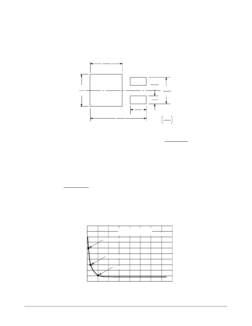
technology. For example, a graph of R
θ
JA versus drain pad
area is shown in Figure 17.
Figure 17. Thermal Resistance versus Drain Pad
Area for the D2PAK Package (Typical)
2.5 Watts
A, AREA (SQUARE INCHES)
Board Material = 0.0625
″
G-10/FR-4, 2 oz Copper
TA = 25
°
C
60
70
50
40
30
20
16
14
12
10
8
6
4
2
0
3.5 Watts
5 Watts
T
°
R
θ
相關(guān)PDF資料 |
PDF描述 |
|---|---|
| MTD20N06HDLT4 | Power MOSFET 20 Amps, 60 Volts, Logic Level N−Channel DPAK |
| MTD20N06HDLT4G | Power MOSFET 20 Amps, 60 Volts, Logic Level N−Channel DPAK |
| MTD6N15 | Power Field Effect Transistor DPAK for Surface Mount(功率場效應(yīng)晶體管) |
| MTD6N20E | Power MOSFET 6 Amps, 200 Volts(6A, 200V功率MOSFET) |
| MTG-12864A | MTG-12864A |
相關(guān)代理商/技術(shù)參數(shù) |
參數(shù)描述 |
|---|---|
| MTB50P03HDLG | 功能描述:MOSFET PFET 30V 50A RoHS:否 制造商:STMicroelectronics 晶體管極性:N-Channel 汲極/源極擊穿電壓:650 V 閘/源擊穿電壓:25 V 漏極連續(xù)電流:130 A 電阻汲極/源極 RDS(導(dǎo)通):0.014 Ohms 配置:Single 最大工作溫度: 安裝風(fēng)格:Through Hole 封裝 / 箱體:Max247 封裝:Tube |
| MTB50P03HDLT4 | 功能描述:MOSFET 30V 50A Logic Level RoHS:否 制造商:STMicroelectronics 晶體管極性:N-Channel 汲極/源極擊穿電壓:650 V 閘/源擊穿電壓:25 V 漏極連續(xù)電流:130 A 電阻汲極/源極 RDS(導(dǎo)通):0.014 Ohms 配置:Single 最大工作溫度: 安裝風(fēng)格:Through Hole 封裝 / 箱體:Max247 封裝:Tube |
| MTB50P03HDLT4G | 功能描述:MOSFET PFET D2PAK 30V 50A 25mOhm RoHS:否 制造商:STMicroelectronics 晶體管極性:N-Channel 汲極/源極擊穿電壓:650 V 閘/源擊穿電壓:25 V 漏極連續(xù)電流:130 A 電阻汲極/源極 RDS(導(dǎo)通):0.014 Ohms 配置:Single 最大工作溫度: 安裝風(fēng)格:Through Hole 封裝 / 箱體:Max247 封裝:Tube |
| MTB50SA | 制造商:未知廠家 制造商全稱:未知廠家 功能描述:Full-Size (7.3mm or 4.7mm height) |
| MTB50SAM | 制造商:未知廠家 制造商全稱:未知廠家 功能描述:Full-Size (7.3mm or 4.7mm height) |
發(fā)布緊急采購,3分鐘左右您將得到回復(fù)。