- 您現(xiàn)在的位置:買賣IC網(wǎng) > PDF目錄384760 > MT9044AP (Mitel Networks Corporation) T1/E1/OC3 System Synchronizer PDF資料下載
參數(shù)資料
| 型號: | MT9044AP |
| 廠商: | Mitel Networks Corporation |
| 英文描述: | T1/E1/OC3 System Synchronizer |
| 中文描述: | T1/E1/OC3系統(tǒng)同步 |
| 文件頁數(shù): | 7/30頁 |
| 文件大小: | 120K |
| 代理商: | MT9044AP |
第1頁第2頁第3頁第4頁第5頁第6頁當(dāng)前第7頁第8頁第9頁第10頁第11頁第12頁第13頁第14頁第15頁第16頁第17頁第18頁第19頁第20頁第21頁第22頁第23頁第24頁第25頁第26頁第27頁第28頁第29頁第30頁
Advance Information
MT9044
7
In Normal Mode, the DCO provides an output signal
which is frequency and phase locked to the selected
input reference signal.
In Holdover Mode, the DCO is free running at a
frequency equal to the last (less 30ms to 60ms)
frequency the DCO was generating while in Normal
Mode.
In Freerun Mode, the DCO is free running with an
accuracy equal to the accuracy of the OSCi 20MHz
source.
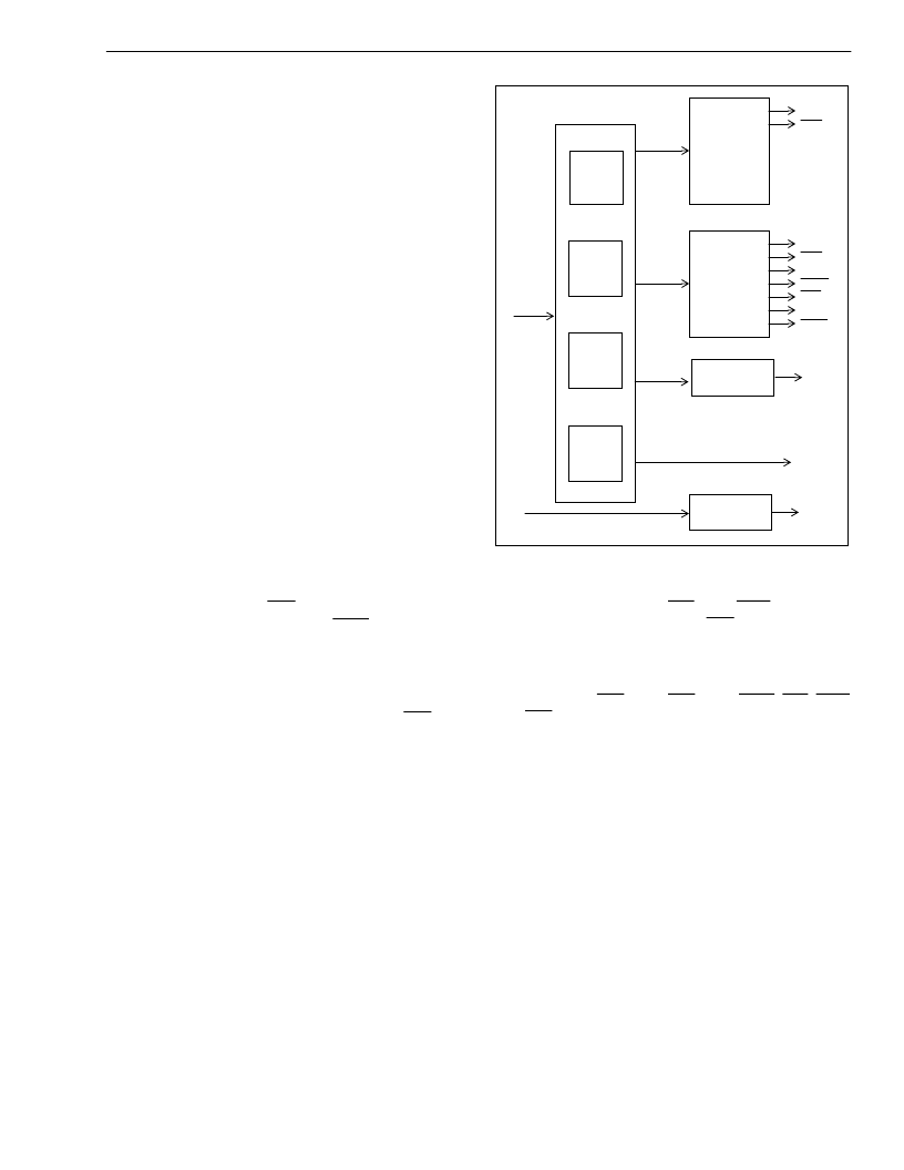
Output Interface Circuit
The output of the DCO (DPLL) is used by the Output
Interface Circuit to provide the output signals shown
in Figure 5. The Output Interface Circuit uses four
Tapped Delay Lines followed by a T1 Divider Circuit ,
an E1 Divider Circuit, a DS2 Divider Circuit and an
analog PLL to generate the required output signals.
Four tapped delay lines are used to generate a
16.384MHz, 12.352MHz, 12.624MHz and 19.44 MHz
signals.
The E1 Divider Circuit uses the 16.384MHz signal to
generate four clock outputs and three frame pulse
outputs. The C8o, C4o and C2o clocks are
generated by simply dividing the C16o clock by two,
four and eight respectively. These outputs have a
nominal 50% duty cycle.
The T1 Divider Circuit uses the 12.384MHz signal to
generate two clock outputs. C1.5o and C3o are
generated by dividing the internal C12 clock by four
and eight respectively. These outputs have a
nominal 50% duty cycle.
The DS2 Divider Circuit uses the 12.624 MHz signal
to generate the clock output C6o. This output has a
nominal 50% duty cycle.
Figure 5 - Output Interface Circuit Block
Diagram
The frame pulse outputs (F0o, F8o, F16o, TSP, RSP)
are generated directly from the C16 clock.
The T1 and E1 signals are generated from a
common DPLL signal. Consequently, the clock
outputs C1.5o, C3o, C2o, C4o, C8o, C16o, F0o, F16o
and C6o are locked to one another for all operating
states, and are also locked to the selected input
reference in Normal Mode. See Figures 20 and 21.
All frame pulse and clock outputs have limited driving
capability, and should be buffered when driving high
capacitance (e.g. 30pF) loads.
Analog Phase Lock Loop (APLL)
The analog PLL is intended to be used to achieve a
50% duty cycle output clock. Connecting C19o to
ACKi will generate a phase locked 19.44 MHz ACKo
output with a nominal 50% duty cycle. The analog
PLL has an intrinsic jitter of less than 0.01 U.I. In
order to achieve this low jitter level a separate pin is
provided to power (AVdd) the analog PLL.
Tapped
Delay
Line
From
DPLL
T1 Divider
E1 Divider
16MHz
12MHz
C3o
C1.5o
C2o
C4o
C8o
C16o
F0o
F8o
F16o
Tapped
Delay
Line
Tapped
Delay
Line
Tapped
Delay
Line
Analog PLL
DS2 Divider
12MHz
19MHz
C6o
C19o
ACKo
ACKi
相關(guān)PDF資料 |
PDF描述 |
|---|---|
| MT9045 | T1/E1/OC3 System Synchronizer(T1/E1/OC3 系統(tǒng)同步裝置(由一個數(shù)字鎖相環(huán)組成)) |
| MT90710 | High-Speed Isochronous Multiplexer |
| MT90710AP | High-Speed Isochronous Multiplexer |
| MT9071 | Quad T1/E1/J1 Transceiver(多端口 T1/E1/J1幀調(diào)節(jié)器(集成四個獨立幀調(diào)節(jié)器)) |
| MT9072 | Ultraframer DS3/E3/DS2/E2/DS1/E1/DS0 |
相關(guān)代理商/技術(shù)參數(shù) |
參數(shù)描述 |
|---|---|
| MT9044AP1 | 制造商:Microsemi Corporation 功能描述:FRAMER E1/OC3/T1 5V 44PLCC - Rail/Tube 制造商:Microsemi Corporation 功能描述:T1/E1/OC3 SYSTEM SYNCHRONIZER 制造商:MICROSEMI CONSUMER MEDICAL PRODUCT GROUP 功能描述:IC SYNCHRONIZER T1/E1 44PLCC 制造商:Microsemi Corporation 功能描述:IC SYNCHRONIZER T1/E1 44PLCC |
| MT9044APR1 | 制造商:Microsemi Corporation 功能描述:FRAMER E1/OC3/T1 5V 44PLCC - Tape and Reel 制造商:Zarlink Semiconductor Inc 功能描述:FRAMER E1/OC3/T1 5V 44PLCC - Tape and Reel |
| MT9045 | 制造商:ZARLINK 制造商全稱:Zarlink Semiconductor Inc 功能描述:T1/E1/OC3 System Synchronizer |
| MT9045AN | 制造商:Microsemi Corporation 功能描述: |
| MT9045AN1 | 制造商:Microsemi Corporation 功能描述:FRAMER E1/OC3/T1 3.3V 48SSOP - Rail/Tube 制造商:Microsemi Corporation 功能描述:T1/E1/OC3 SYSTEM SYNCHRONIZER |
發(fā)布緊急采購,3分鐘左右您將得到回復(fù)。