- 您現(xiàn)在的位置:買賣IC網(wǎng) > PDF目錄384755 > MT48LC4M32LFFC (Micron Technology, Inc.) SYNCHRONOUS DRAM PDF資料下載
參數(shù)資料
| 型號(hào): | MT48LC4M32LFFC |
| 廠商: | Micron Technology, Inc. |
| 英文描述: | SYNCHRONOUS DRAM |
| 中文描述: | 同步DRAM |
| 文件頁數(shù): | 23/52頁 |
| 文件大小: | 1281K |
| 代理商: | MT48LC4M32LFFC |
第1頁第2頁第3頁第4頁第5頁第6頁第7頁第8頁第9頁第10頁第11頁第12頁第13頁第14頁第15頁第16頁第17頁第18頁第19頁第20頁第21頁第22頁當(dāng)前第23頁第24頁第25頁第26頁第27頁第28頁第29頁第30頁第31頁第32頁第33頁第34頁第35頁第36頁第37頁第38頁第39頁第40頁第41頁第42頁第43頁第44頁第45頁第46頁第47頁第48頁第49頁第50頁第51頁第52頁
23
128Mb: x32 SDRAM
128MbSDRAMx32_D.p65 – Rev. D; Pub. 6/02
Micron Technology, Inc., reserves the right to change products or specifications without notice.
2002, Micron Technology, Inc.
128Mb: x32
SDRAM
DON’T CARE
D
IN
COMMAND
ADDRESS
WRITE
BANK,
COL
n
D
IN
n
NOP
NOP
CLK
T2
T1
T4
T3
T5
T0
CKE
INTERNAL
CLOCK
NOP
D
IN
n
+ 1
D
IN
n
+ 2
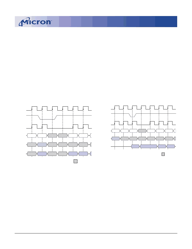
Figure 22
CLOCK SUSPEND During WRITE Burst
DON’T CARE
CLK
DQ
D
OUT
n
T2
T1
T4
T3
T6
T5
T0
COMMAND
ADDRESS
READ
NOP
NOP
NOP
BANK,
COL
n
NOP
D
OUT
n
+ 1
D
OUT
n
+ 2
D
OUT
n
+ 3
NOTE:
For this example, CAS latency = 2, burst length = 4 or greater, and
DQM is LOW.
CKE
INTERNAL
CLOCK
NOP
Figure 23
CLOCK SUSPEND During READ Burst
CLOCK SUSPEND
The clock suspend mode occurs when a column ac-
cess/burst is in progress and CKE is registered LOW. In
the clock suspend mode, the internal clock is deacti-
vated, “freezing” the synchronous logic.
For each positive clock edge on which CKE is
sampled LOW, the next internal positive clock edge is
suspended. Any command or data present on the in-
put pins at the time of a suspended internal clock edge
is ignored; any data present on the DQ pins remains
driven; and burst counters are not incremented, as
long as the clock is suspended. (See examples in Fig-
ures 22 and 23.)
Clock suspend mode is exited by registering CKE
HIGH; the internal clock and related operation will re-
sume on the subsequent positive clock edge.
BURST READ/SINGLE WRITE
The burst read/single write mode is entered by pro-
gramming the write burst mode bit (M9) in the Mode
Register to a logic 1. In this mode, all WRITE commands
result in the access of a single column location (burst of
one), regardless of the programmed burst length. READ
commands access columns according to the pro-
grammed burst length and sequence, just as in the
normal mode of operation (M9 = 0).
相關(guān)PDF資料 |
PDF描述 |
|---|---|
| MT48LC64M8A2 | SYNCHRONOUS DRAM |
| MT48LC32M16A2 | SYNCHRONOUS DRAM |
| MT48LC8M16A2FB-75LIT | SYNCHRONOUS DRAM |
| MT48LC8M16A2FB-7E | SYNCHRONOUS DRAM |
| MT48LC8M16A2FB-7EIT | SYNCHRONOUS DRAM |
相關(guān)代理商/技術(shù)參數(shù) |
參數(shù)描述 |
|---|---|
| MT48LC4M32LFFC-10-REFURB | 制造商:Micron Technology Inc 功能描述: |
| MT48LC4M4A1 | 制造商:MICRON 制造商全稱:Micron Technology 功能描述:SYNCHRONOUS DRAM |
| MT48LC4M4A1TGS | 制造商:MICRON 制造商全稱:Micron Technology 功能描述:SYNCHRONOUS DRAM |
| MT48LC4M4A2 | 制造商:MICRON 制造商全稱:Micron Technology 功能描述:SYNCHRONOUS DRAM |
| MT48LC64M4A2 | 制造商:MICRON 制造商全稱:Micron Technology 功能描述:SYNCHRONOUS DRAM |
發(fā)布緊急采購,3分鐘左右您將得到回復(fù)。