- 您現(xiàn)在的位置:買賣IC網(wǎng) > PDF目錄384755 > MT48LC4M32LFFC (Micron Technology, Inc.) SYNCHRONOUS DRAM PDF資料下載
參數(shù)資料
| 型號(hào): | MT48LC4M32LFFC |
| 廠商: | Micron Technology, Inc. |
| 英文描述: | SYNCHRONOUS DRAM |
| 中文描述: | 同步DRAM |
| 文件頁(yè)數(shù): | 17/52頁(yè) |
| 文件大小: | 1281K |
| 代理商: | MT48LC4M32LFFC |
第1頁(yè)第2頁(yè)第3頁(yè)第4頁(yè)第5頁(yè)第6頁(yè)第7頁(yè)第8頁(yè)第9頁(yè)第10頁(yè)第11頁(yè)第12頁(yè)第13頁(yè)第14頁(yè)第15頁(yè)第16頁(yè)當(dāng)前第17頁(yè)第18頁(yè)第19頁(yè)第20頁(yè)第21頁(yè)第22頁(yè)第23頁(yè)第24頁(yè)第25頁(yè)第26頁(yè)第27頁(yè)第28頁(yè)第29頁(yè)第30頁(yè)第31頁(yè)第32頁(yè)第33頁(yè)第34頁(yè)第35頁(yè)第36頁(yè)第37頁(yè)第38頁(yè)第39頁(yè)第40頁(yè)第41頁(yè)第42頁(yè)第43頁(yè)第44頁(yè)第45頁(yè)第46頁(yè)第47頁(yè)第48頁(yè)第49頁(yè)第50頁(yè)第51頁(yè)第52頁(yè)
17
128Mb: x32 SDRAM
128MbSDRAMx32_D.p65 – Rev. D; Pub. 6/02
Micron Technology, Inc., reserves the right to change products or specifications without notice.
2002, Micron Technology, Inc.
128Mb: x32
SDRAM
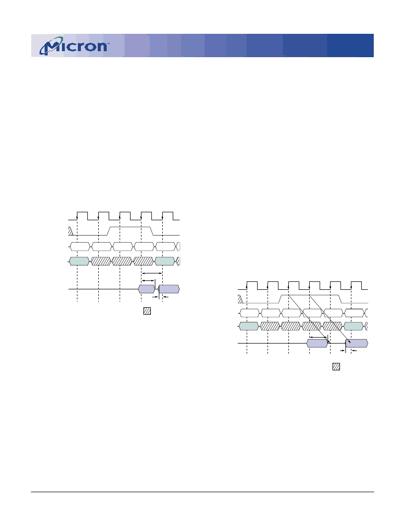
Data from any READ burst may be truncated with a
subsequent WRITE command, and data from a fixed-
length READ burst may be immediately followed by
data from a WRITE command (subject to bus turn-
around limitations). The WRITE burst may be initiated
on the clock edge immediately following the last (or last
desired) data element from the READ burst, provided
that I/O contention can be avoided. In a given system
design, there may be a possibility that the device driv-
ing the input data will go Low-Z before the SDRAM DQs
go High-Z. In this case, at least a single-cycle delay
should occur between the last read data and the WRITE
command.
DON’T CARE
READ
NOP
NOP
NOP
NOP
DQM
CLK
DQ
D
OUT
n
T2
T1
T4
T3
T0
COMMAND
ADDRESS
BANK,
COL
n
WRITE
D
IN
b
BANK,
COL
b
T5
DS
t
HZ
t
NOTE:
A CAS latency of three is used for illustration. The
READ command
may be to any bank, and the WRITE command may be to any bank.
Figure 10
READ to WRITE with
Extra Clock Cycle
Figure 9
READ to WRITE
DON’T CARE
READ
NOP
NOP
WRITE
NOP
CLK
T2
T1
T4
T3
T0
DQM
DQ
D
OUT
n
COMMAND
D
IN
b
ADDRESS
COL
n
COL
b
DS
t
HZ
t
t
CK
NOTE:
A CAS latency of three is used for illustration. The
READ
command may be to any bank, and the WRITE command
may be to any bank. If a burst of one is used, then DQM is
not required.
The DQM input is used to avoid I/O contention, as
shown in Figures 9 and 10. The DQM signal must be
asserted (HIGH) at least two clocks prior to the WRITE
command (DQM latency is two clocks for output buff-
ers) to suppress data-out from the READ. Once the
WRITE command is registered, the DQs will go High-Z
(or remain High-Z), regardless of the state of the DQM
signal; provided the DQM was active on the clock just
prior to the WRITE command that truncated the READ
command. If not, the second WRITE will be an invalid
WRITE. For example, if DQM was low during T4 in Fig-
ure 10, then the WRITEs at T5 and T7 would be valid,
while the WRITE at T6 would be invalid.
The DQM signal must be de-asserted prior to the
WRITE command (DQM latency is zero clocks for input
buffers) to ensure that the written data is not masked.
Figure 9 shows the case where the clock frequency al-
lows for bus contention to be avoided without adding a
NOP cycle, and Figure 10 shows the case where the
additional NOP is needed.
相關(guān)PDF資料 |
PDF描述 |
|---|---|
| MT48LC64M8A2 | SYNCHRONOUS DRAM |
| MT48LC32M16A2 | SYNCHRONOUS DRAM |
| MT48LC8M16A2FB-75LIT | SYNCHRONOUS DRAM |
| MT48LC8M16A2FB-7E | SYNCHRONOUS DRAM |
| MT48LC8M16A2FB-7EIT | SYNCHRONOUS DRAM |
相關(guān)代理商/技術(shù)參數(shù) |
參數(shù)描述 |
|---|---|
| MT48LC4M32LFFC-10-REFURB | 制造商:Micron Technology Inc 功能描述: |
| MT48LC4M4A1 | 制造商:MICRON 制造商全稱:Micron Technology 功能描述:SYNCHRONOUS DRAM |
| MT48LC4M4A1TGS | 制造商:MICRON 制造商全稱:Micron Technology 功能描述:SYNCHRONOUS DRAM |
| MT48LC4M4A2 | 制造商:MICRON 制造商全稱:Micron Technology 功能描述:SYNCHRONOUS DRAM |
| MT48LC64M4A2 | 制造商:MICRON 制造商全稱:Micron Technology 功能描述:SYNCHRONOUS DRAM |
發(fā)布緊急采購(gòu),3分鐘左右您將得到回復(fù)。