- 您現(xiàn)在的位置:買賣IC網(wǎng) > PDF目錄384755 > MT48LC32M16A2 (Micron Technology, Inc.) SYNCHRONOUS DRAM PDF資料下載
參數(shù)資料
| 型號: | MT48LC32M16A2 |
| 廠商: | Micron Technology, Inc. |
| 英文描述: | SYNCHRONOUS DRAM |
| 中文描述: | 同步DRAM |
| 文件頁數(shù): | 1/55頁 |
| 文件大小: | 1828K |
| 代理商: | MT48LC32M16A2 |
當(dāng)前第1頁第2頁第3頁第4頁第5頁第6頁第7頁第8頁第9頁第10頁第11頁第12頁第13頁第14頁第15頁第16頁第17頁第18頁第19頁第20頁第21頁第22頁第23頁第24頁第25頁第26頁第27頁第28頁第29頁第30頁第31頁第32頁第33頁第34頁第35頁第36頁第37頁第38頁第39頁第40頁第41頁第42頁第43頁第44頁第45頁第46頁第47頁第48頁第49頁第50頁第51頁第52頁第53頁第54頁第55頁
ADVANCE
PRODUCTS AND SPECIFICATIONS DISCUSSED HEREIN ARE FOR EVALUATION AND REFERENCE PURPOSES ONLY AND ARE SUBJECT TO CHANGE
BY MICRON WITHOUT NOTICE. PRODUCTS ARE ONLY WARRANTED BY MICRON TO MEET MICRON’S PRODUCTION DATA SHEET SPECIFICATIONS.
1
512Mb: x4, x8, x16
SDRAM
512Mb: x4, x8, x16 SDRAM
512MSDRAM_D.p65 – Rev. D; Pub 1/02
Micron Technology, Inc., reserves the right to change products or specifications without notice.
2000, Micron Technology, Inc.
KEY TIMING PARAMETERS
SPEED
GRADE
-7E
-75
-7E
-75
CLOCK
FREQUENCY CL = 2* CL = 3*
143 MHz
133 MHz
133 MHz
100 MHz
ACCESS TIME
SETUP
TIME
1.5ns
1.5ns
1.5ns
1.5ns
HOLD
TIME
0.8ns
0.8ns
0.8ns
0.8ns
–
–
5.4ns
5.4ns
–
–
5.4ns
6ns
128 Meg x 4
32 Meg x 4 x 4 banks 16 Meg x 8 x 4 banks 8 Meg x 16 x 4 banks
8K
8K
8K (A0–A12)
8K (A0–A12)
4 (BA0, BA1)
4 (BA0, BA1)
Column Addressing 4K (A0–A9, A11, A12)
64 Meg x 8
32 Meg x 16
Configuration
Refresh Count
Row Addressing
Bank Addressing
8K
8K (A0–A12)
4 (BA0, BA1)
1K (A0–A9)
2K (A0–A9, A11)
SYNCHRONOUS
DRAM
MT48LC128M4A2 – 32 Meg x 4
MT48LC64M8A2 – 16 Meg x 8
MT48LC32M16A2 – 8 Meg x 16 x 4 banks
For the latest data sheet, please refer to the Micron Web site:
x 4 banksx 4 banks
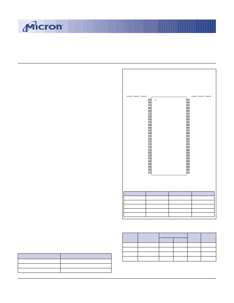
Pin Assignment (Top View)
54-Pin TSOP
FEATURES
PC100- and PC133-compliant
Fully synchronous; all signals registered on positive
edge of system clock
Internal pipelined operation; column address can be
changed every clock cycle
Internal banks for hiding row access/precharge
Programmable burst lengths: 1, 2, 4, 8, or full page
Auto Precharge, includes CONCURRENT AUTO
PRECHARGE, and Auto Refresh Modes
Self Refresh Mode
64ms, 8,192-cycle refresh
LVTTL-compatible inputs and outputs
Single +3.3V ±0.3V power supply
OPTIONS
Configurations
128 Meg x 4
64 Meg x 8
32 Meg x 16
WRITE Recovery (
t
WR)
t
WR = “2 CLK”
1
Plastic Package – OCPL
2
54-pin TSOP II (400 mil)
Timing (Cycle Time)
7.5ns @ CL = 2 (PC133)
7.5ns @ CL = 3 (PC133)
Self Refresh
Standard
Low power
Operating Temperature
Commercial (0
o
C to +70
o
C)
MARKING
(32 Meg x 4 x 4 banks)
(16 Meg x 8 x 4 banks)
(8 Meg x 16 x 4 banks)
128M4
64M8
32M16
A2
TG
-7E
-75
None
L
None
NOTE:
1. Refer to Micron Technical Note TN-48-05.
2. Off-center parting line.
Part Number Example:
MT48LC32M16A2TG-75
NOTE:
The # symbol indicates signal is active LOW. A dash
(–) indicates x8 and x4 pin function is same as x16
pin function.
V
DD
DQ0
V
DD
Q
DQ1
DQ2
VssQ
DQ3
DQ4
V
DD
Q
DQ5
DQ6
VssQ
DQ7
V
DD
DQML
WE#
CAS#
RAS#
CS#
BA0
BA1
A10
A0
A1
A2
A3
V
DD
1
2
3
4
5
6
7
8
9
10
11
12
13
14
15
16
17
18
19
20
21
22
23
24
25
26
27
54
53
52
51
50
49
48
47
46
45
44
43
42
41
40
39
38
37
36
35
34
33
32
31
30
29
28
Vss
DQ15
VssQ
DQ14
DQ13
V
DD
Q
DQ12
DQ11
VssQ
DQ10
DQ9
V
DD
Q
DQ8
Vss
NC
DQMH
CLK
CKE
A12
A11
A9
A8
A7
A6
A5
A4
Vss
x8
-
DQ7
-
NC
DQ6
-
NC
DQ5
-
NC
DQ4
-
NC
-
-
DQM
-
-
-
-
-
-
-
-
-
-
-
x16
x16
x8
-
DQ0
-
NC
DQ1
-
NC
DQ2
-
NC
DQ3
-
NC
-
NC
-
-
-
-
-
-
-
-
-
-
-
-
x4
-
NC
-
NC
DQ3
-
NC
NC
-
NC
DQ2
-
NC
-
-
DQM
-
-
-
-
-
-
-
-
-
-
-
x4
-
NC
-
NC
DQ0
-
NC
NC
-
NC
DQ1
-
NC
-
NC
-
-
-
-
-
-
-
-
-
-
-
-
*CL = CAS (READ) latency
512Mb SDRAM PART NUMBERS
PART NUMBER
MT48LC128M4A2TG
MT48LC64M8A2TG
MT48LC32M16A2TG
ARCHITECTURE
128 Meg x 4
64 Meg x 8
32 Meg x 16
相關(guān)PDF資料 |
PDF描述 |
|---|---|
| MT48LC8M16A2FB-75LIT | SYNCHRONOUS DRAM |
| MT48LC8M16A2FB-7E | SYNCHRONOUS DRAM |
| MT48LC8M16A2FB-7EIT | SYNCHRONOUS DRAM |
| MT48LC8M16A2FB-7EL | SYNCHRONOUS DRAM |
| MT48LC8M16A2FB-7ELIT | SYNCHRONOUS DRAM |
相關(guān)代理商/技術(shù)參數(shù) |
參數(shù)描述 |
|---|---|
| MT48LC32M16A2-75ITC | 制造商:Micron Technology Inc 功能描述: |
| MT48LC32M16A2P-75 | 制造商:Micron Technology Inc 功能描述: |
| MT48LC32M16A2P-75 C TR | 制造商:Micron Technology Inc 功能描述:DRAM Chip SDRAM 512M-Bit 32Mx16 3.3V 54-Pin TSOP-II T/R 制造商:Micron Technology 功能描述:DRAM Chip SDRAM 512M-Bit 32Mx16 3.3V 54-Pin TSOP-II T/R |
發(fā)布緊急采購,3分鐘左右您將得到回復(fù)。