- 您現(xiàn)在的位置:買賣IC網(wǎng) > PDF目錄371135 > MPC992 (Motorola, Inc.) Low Voltage PLL Clock Driver(低壓PLL時(shí)鐘驅(qū)動(dòng)器) PDF資料下載
參數(shù)資料
| 型號(hào): | MPC992 |
| 廠商: | Motorola, Inc. |
| 英文描述: | Low Voltage PLL Clock Driver(低壓PLL時(shí)鐘驅(qū)動(dòng)器) |
| 中文描述: | 低電壓PLL時(shí)鐘驅(qū)動(dòng)器(低壓鎖相環(huán)時(shí)鐘驅(qū)動(dòng)器) |
| 文件頁數(shù): | 5/8頁 |
| 文件大小: | 104K |
| 代理商: | MPC992 |

MPC992
TIMING SOLUTIONS
BR1333 — REV 5
5
MOTOROLA
a parallel specified crystal used in a series resonant mode
will exhibit an oscillatory frequency a few hundred ppm lower
than the specified value. For most processor implementa–
tions a few hundred ppm translates into kHz inaccuracies, a
level which does not represent a major issue.
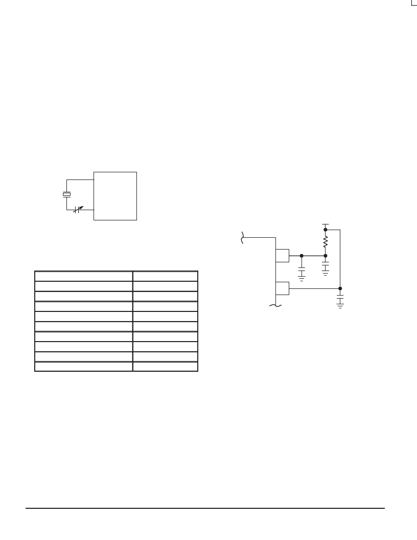
Figure 2 shows an optional series capacitor in the crystal
oscillator interface. The on–board oscillator introduces a
small phase shift in the overall loop which causes the
oscillator to operate at a frequency slightly slower than the
specified crystal. The series capacitor is used to compensate
the loop and allow the oscillator to function at the specified
crystal frequency. If a 100ppm type error is not important, the
capacitor can be left off the PCB. For more detailed
information, order Motorola Application Note AN1579/D.
Figure 2. Recommended Crystal Interface
XTAL2
CTUNE
(Optional)
XTAL1
MPC992
Table 1. Crystal Specifications
Parameter
Value
Crystal Cut
Fundamental AT Cut
Resonance
Series Resonance*
Frequency Tolerance
±
75ppm at 25
°
C
Frequency/Temperature Stability
±
150ppm 0 to 70
°
C
Operating Range
0 to 70
°
C
Shunt Capacitance
5–7pF
Equivalent Series Resistance (ESR)
50 to 80
max
Correlation Drive Level
100
μ
W
Aging
5ppm/Yr (First 3 Years)
Power Supply Filtering
The MPC992 is a mixed analog/digital product and as
such it exhibits some sensitivities that would not necessarily
be seen on a fully digital product. Analog circuitry is naturally
susceptible to random noise, especially if this noise is seen
on the power supply pins. The MPC992 provides separate
power supplies for the digital circuitry (VCCI) and the internal
PLL (VCCA) of the device. The purpose of this design
technique is to try and isolate the high switching noise digital
outputs from the relatively sensitive internal analog
phase–locked loop. In a controlled environment such as an
evaluation board this level of isolation is sufficient. However,
in a digital system environment where it is more difficult to
minimize noise on the power supplies a second level of
isolation may be required. The simplest form of isolation is a
power supply filter on the VCCA pin for the MPC992.
Figure 3 illustrates a typical power supply filter scheme.
The MPC992 is most susceptible to noise with spectral
content in the 10kHz to 1MHz range. Therefore the filter
should be designed to target this range. The key parameter
that needs to be met in the final filter design is the DC voltage
drop that will be seen between the VCC supply and the VCCA
pin of the MPC992. From the data sheet the IVCCA current
(the current sourced through the VCCA pin) is typically 15mA
(20mA maximum), assuming that a minimum of 3.0V must be
maintained on the VCCA pin very little DC voltage drop can
be tolerated when a 3.3V VCC supply is used. The resistor
shown in Figure 3 must have a resistance of 10–15
to meet
the voltage drop criteria. The RC filter pictured will provide a
broadband filter with approximately 100:1 attenuation for
noise whose spectral content is above 20KHz. As the noise
frequency crosses the series resonant point of an individual
capacitor it’s overall impedance begins to look inductive and
thus increases with increasing frequency. The parallel
capacitor combination shown ensures that a low impedance
path to ground exists for frequencies well above the
bandwidth of the PLL.
Figure 3. Power Supply Filter
VCCA
VCC
MPC992
0.01
μ
F
22
μ
F
0.01
μ
F
3.3V
RS=10–15
A higher level of attenuation can be achieved by replacing
the resistor with an appropriate valued inductor. A 1000
μ
H
choke will show a significant impedance at 10KHz
frequencies and above. Because of the current draw and the
voltage that must be maintained on the VCCA pin a low DC
resistance inductor is required (less than 15
). Generally the
resistor/capacitor filter will be cheaper, easier to implement
and provide an adequate level of supply filtering.
The MPC992 provides sub–nanosecond output edge
rates and thus a good power supply bypassing scheme is a
must. The important aspect of the layout for the MPC992 is
low impedance connections between VCC and GND for the
bypass capacitors. Combining good quality general purpose
chip capacitors with good PCB layout techniques will
produce effective capacitor resonances at frequencies
adequate to supply the instantaneous switching current for
the MPC992 outputs. It is imperative that low inductance chip
capacitors are used; it is equally important that the board
layout does not introduce back all of the inductance saved by
using the leadless capacitors. Thin interconnect traces
between the capacitor and the power plane should be
avoided and multiple large vias should be used to tie the
相關(guān)PDF資料 |
PDF描述 |
|---|---|
| MPC993 | Dynamic Switch PLL Clock Driver(動(dòng)態(tài)開關(guān)PLL時(shí)鐘驅(qū)動(dòng)器) |
| MPC9990 | Low Voltage PLL Clock Driver(低壓PLL時(shí)鐘驅(qū)動(dòng)器) |
| MPF102 | JFET VHF Amplifier |
| MPF102 | JFET VHF Amplifier |
| MPF102 | N-Channel RF Amplifier |
相關(guān)代理商/技術(shù)參數(shù) |
參數(shù)描述 |
|---|---|
| MPC992D33 F44A WAF | 制造商:Motorola Inc 功能描述: |
| MPC993 | 制造商:MOTOROLA 制造商全稱:Motorola, Inc 功能描述:Dynamic Switch PLL Clock Driver |
| MPC9992 | 制造商:MOTOROLA 制造商全稱:Motorola, Inc 功能描述:3.3 DIFFRERENTIAL ECL/PECL PLL CLOCK GENERATOR |
| MPC9992AC | 功能描述:時(shí)鐘發(fā)生器及支持產(chǎn)品 RoHS:否 制造商:Silicon Labs 類型:Clock Generators 最大輸入頻率:14.318 MHz 最大輸出頻率:166 MHz 輸出端數(shù)量:16 占空比 - 最大:55 % 工作電源電壓:3.3 V 工作電源電流:1 mA 最大工作溫度:+ 85 C 安裝風(fēng)格:SMD/SMT 封裝 / 箱體:QFN-56 |
| MPC9992ACR2 | 功能描述:時(shí)鐘發(fā)生器及支持產(chǎn)品 RoHS:否 制造商:Silicon Labs 類型:Clock Generators 最大輸入頻率:14.318 MHz 最大輸出頻率:166 MHz 輸出端數(shù)量:16 占空比 - 最大:55 % 工作電源電壓:3.3 V 工作電源電流:1 mA 最大工作溫度:+ 85 C 安裝風(fēng)格:SMD/SMT 封裝 / 箱體:QFN-56 |
發(fā)布緊急采購,3分鐘左右您將得到回復(fù)。