- 您現(xiàn)在的位置:買賣IC網(wǎng) > PDF目錄371135 > MPC992 (Motorola, Inc.) Low Voltage PLL Clock Driver(低壓PLL時鐘驅(qū)動器) PDF資料下載
參數(shù)資料
| 型號: | MPC992 |
| 廠商: | Motorola, Inc. |
| 英文描述: | Low Voltage PLL Clock Driver(低壓PLL時鐘驅(qū)動器) |
| 中文描述: | 低電壓PLL時鐘驅(qū)動器(低壓鎖相環(huán)時鐘驅(qū)動器) |
| 文件頁數(shù): | 4/8頁 |
| 文件大?。?/td> | 104K |
| 代理商: | MPC992 |
MPC992
MOTOROLA
TIMING SOLUTIONS
BR1333 — REV 5
4
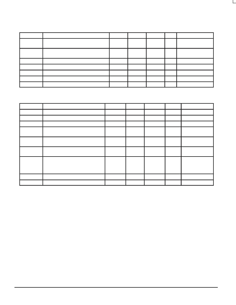
DC CHARACTERISTICS
(TA = 0
°
to 70
°
C, VCC = 3.3V
±
5%)
Symbol
Characteristic
Min
Typ
Max
Unit
Condition
VIH
Input HIGH Voltage
PECL_CLK
1
Other
2.15
2.0
2.4
VCC
V
VCC = 3.3V
VIL
Input LOW Voltage
PECL_CLK
1
Other
1.5
0
1.8
0.8
V
VCC = 3.3V
VOH
VOL
IIN
ICCI
ICCA
1. DC levels will vary 1:1 with VCC.
Output HIGH Voltage
1
Output LOW Voltage
1
1.8
2.4
V
VCC = 3.3V
VCC = 3.3V
1.2
1.7
V
Input Current
–120
120
μ
A
Maximum Quiescent Supply Current
130
150
mA
Maximum PLL Supply Current
15
20
mA
AC CHARACTERISTICS
(TA = 0
°
to 70
°
C, VCC = 3.3V
±
5%)
Symbol
Characteristic
Min
Typ
Max
Unit
Condition
tr, tf
tpw1
tpw2
fref
Output Rise/Fall Time
200
850
ps
20% to 80%
Output Duty Cycle
49
51
%
SYNC Output Duty Cycle
0.95
1.05
%
PCLK Period
Input Reference Frequency
Xtal
FREF
10
Note 2
20
Note 2
MHz
tos
Output-to-Output Skew
Qa, Qb
Qa (–) to SYNC (+)
100
300
ps
fVCO
PLL VCO Lock Range
200
400
440
750
MHz
VCO_SEL = 1
VCO_SEL = 0
fmax
Maximum Output Frequency
Qa (
÷
2)
Qa,Qb (
÷
4)
Qb (
÷
6)
Qb (
÷
10)
375
187.5
125
75
MHz
Note 1
tjitter
tlock
1. At 400MHz the output swing will be less than the nominal value.
2. ECLK and XTAL input reference limited by the feedback divide and the guaranteed VCO lock range.
3. Guaranteed by characterization.
Cycle–to–Cycle Jitter (Peak–to–Peak)
±
25
±
50
ps
Note 3
Maximum PLL Lock Time
10
ms
APPLICATIONS INFORMATION
Using the On–Board Crystal Oscillator
The MPC992 features an on–board crystal oscillator to
allow for seed clock generation as well as final distribution.
The on–board oscillator is completely self contained so that
the only external component required is the crystal. As the
oscillator is somewhat sensitive to loading on its inputs the
user is advised to mount the crystal as close to the MPC992
as possible to avoid any board level parasitics. To facilitate
co–location surface mount crystals are recommended, but
not required.
The oscillator circuit is a series resonant circuit as
opposed to the more common parallel resonant circuit, this
eliminates the need for large on–board capacitors. Because
the design is a series resonant design, for optimum
frequency accuracy a series resonant crystal should be used
(see specification table below). Unfortunately most off the
shelf crystals are characterized in a parallel resonant mode.
However a parallel resonant crystal is physically no different
than a series resonant crystal, a parallel resonant crystal is
simply a crystal which has been characterized in its parallel
resonant mode. Therefore in the majority of cases a parallel
specified crystal can be used with the MPC992 with just a
minor frequency error due to the actual series resonant
frequency of the parallel resonant specified crystal. Typically
相關(guān)PDF資料 |
PDF描述 |
|---|---|
| MPC993 | Dynamic Switch PLL Clock Driver(動態(tài)開關(guān)PLL時鐘驅(qū)動器) |
| MPC9990 | Low Voltage PLL Clock Driver(低壓PLL時鐘驅(qū)動器) |
| MPF102 | JFET VHF Amplifier |
| MPF102 | JFET VHF Amplifier |
| MPF102 | N-Channel RF Amplifier |
相關(guān)代理商/技術(shù)參數(shù) |
參數(shù)描述 |
|---|---|
| MPC992D33 F44A WAF | 制造商:Motorola Inc 功能描述: |
| MPC993 | 制造商:MOTOROLA 制造商全稱:Motorola, Inc 功能描述:Dynamic Switch PLL Clock Driver |
| MPC9992 | 制造商:MOTOROLA 制造商全稱:Motorola, Inc 功能描述:3.3 DIFFRERENTIAL ECL/PECL PLL CLOCK GENERATOR |
| MPC9992AC | 功能描述:時鐘發(fā)生器及支持產(chǎn)品 RoHS:否 制造商:Silicon Labs 類型:Clock Generators 最大輸入頻率:14.318 MHz 最大輸出頻率:166 MHz 輸出端數(shù)量:16 占空比 - 最大:55 % 工作電源電壓:3.3 V 工作電源電流:1 mA 最大工作溫度:+ 85 C 安裝風(fēng)格:SMD/SMT 封裝 / 箱體:QFN-56 |
| MPC9992ACR2 | 功能描述:時鐘發(fā)生器及支持產(chǎn)品 RoHS:否 制造商:Silicon Labs 類型:Clock Generators 最大輸入頻率:14.318 MHz 最大輸出頻率:166 MHz 輸出端數(shù)量:16 占空比 - 最大:55 % 工作電源電壓:3.3 V 工作電源電流:1 mA 最大工作溫度:+ 85 C 安裝風(fēng)格:SMD/SMT 封裝 / 箱體:QFN-56 |
發(fā)布緊急采購,3分鐘左右您將得到回復(fù)。