- 您現(xiàn)在的位置:買(mǎi)賣IC網(wǎng) > PDF目錄45339 > MPC5606SEMLQR (FREESCALE SEMICONDUCTOR INC) 32-BIT, FLASH, 64 MHz, MICROCONTROLLER, PQFP144 PDF資料下載
參數(shù)資料
| 型號(hào): | MPC5606SEMLQR |
| 廠商: | FREESCALE SEMICONDUCTOR INC |
| 元件分類: | 微控制器/微處理器 |
| 英文描述: | 32-BIT, FLASH, 64 MHz, MICROCONTROLLER, PQFP144 |
| 封裝: | 20 X 20 MM, 1.40 MM HEIGHT, 0.50 MM PITCH, LQFP-144 |
| 文件頁(yè)數(shù): | 42/104頁(yè) |
| 文件大?。?/td> | 1729K |
| 代理商: | MPC5606SEMLQR |
第1頁(yè)第2頁(yè)第3頁(yè)第4頁(yè)第5頁(yè)第6頁(yè)第7頁(yè)第8頁(yè)第9頁(yè)第10頁(yè)第11頁(yè)第12頁(yè)第13頁(yè)第14頁(yè)第15頁(yè)第16頁(yè)第17頁(yè)第18頁(yè)第19頁(yè)第20頁(yè)第21頁(yè)第22頁(yè)第23頁(yè)第24頁(yè)第25頁(yè)第26頁(yè)第27頁(yè)第28頁(yè)第29頁(yè)第30頁(yè)第31頁(yè)第32頁(yè)第33頁(yè)第34頁(yè)第35頁(yè)第36頁(yè)第37頁(yè)第38頁(yè)第39頁(yè)第40頁(yè)第41頁(yè)當(dāng)前第42頁(yè)第43頁(yè)第44頁(yè)第45頁(yè)第46頁(yè)第47頁(yè)第48頁(yè)第49頁(yè)第50頁(yè)第51頁(yè)第52頁(yè)第53頁(yè)第54頁(yè)第55頁(yè)第56頁(yè)第57頁(yè)第58頁(yè)第59頁(yè)第60頁(yè)第61頁(yè)第62頁(yè)第63頁(yè)第64頁(yè)第65頁(yè)第66頁(yè)第67頁(yè)第68頁(yè)第69頁(yè)第70頁(yè)第71頁(yè)第72頁(yè)第73頁(yè)第74頁(yè)第75頁(yè)第76頁(yè)第77頁(yè)第78頁(yè)第79頁(yè)第80頁(yè)第81頁(yè)第82頁(yè)第83頁(yè)第84頁(yè)第85頁(yè)第86頁(yè)第87頁(yè)第88頁(yè)第89頁(yè)第90頁(yè)第91頁(yè)第92頁(yè)第93頁(yè)第94頁(yè)第95頁(yè)第96頁(yè)第97頁(yè)第98頁(yè)第99頁(yè)第100頁(yè)第101頁(yè)第102頁(yè)第103頁(yè)第104頁(yè)
MPC560xS Microcontroller Data Sheet, Rev. 2
Preliminary—Subject to Change Without Notice
Electrical Characteristics
Freescale Semiconductor
42
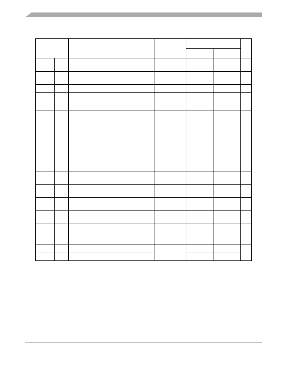
VSSR
SR C Voltage on VSSR (regulator ground) pin with
respect to VSS
VSS 0.1
VSS + 0.1
V
VDD12
3,4 CC C Voltage on VDD12 pin with respect to ground
(VSS12)
1.08
1.4
V
VSS12
CC C Voltage on VSS12 pin with respect to VSS
VSS 0.1
VSS + 0.1
V
VDD
5,6,7
SR C Voltage on VDD pins (VDDE_A, VDDE_B,
VDDE_C, VDDE_E, VDDMA, VDDMB,
VDDMC) with respect to ground (VSS)
3.0
3.6
V
VSS
8
SR C I/O supply ground
0
V
VDDE_A SR C Voltage on VDDE_A (I/O supply) pin with
respect to ground (VSSE_A)
3.0
3.6
V
VDDE_B SR C Voltage on VDDE_B (I/O supply) pin with
respect to ground (VSSE_B)
3.0
3.6
V
VDDE_C
9 SR C Voltage on VDDE_C (I/O supply) pin with
respect to ground (VSSE_C)
3.0
3.6
V
VDDE_E SR C Voltage on VDDE_E (I/O supply) pin with
respect to ground (VSSE_E)
3.0
3.6
V
VDDMA SR C Voltage on VDDMA (stepper motor supply)
pin with respect to ground (VSSMA)
3.0
3.6
V
VDDMB SR C Voltage on VDDMB (stepper motor supply)
pin with respect to ground (VSSMB)
3.0
3.6
V
VDDMC SR C Voltage on VDDMC (stepper motor supply)
pin with respect to ground (VSSMC)
3.0
3.6
V
VSSOSC SR C Voltage on VSSOSC (oscillator ground) pin
with respect to VSS
00
V
VLCD
SR C Voltage on VLCD (LCD supply) pin with
respect to VSS
0VDDE_A + 0.3
V
TVDD
SR C VDD slope to ensure correct power up
10
5 V/s
0.25
V/s
TA
SR C Ambient temperature under bias
40
105
°C
TJ
SR C Junction temperature under bias
40
150
1 100 nF capacitance needs to be provided between V
DDA/VSSA pair.
2 200 F capacitance must be connected between V
DDR and VSS12. This is required because of sharp surge due to
external ballast.
3 V
DD12 cannot be used to drive any external component.
4 Each V
DD12/VSS12 supply pair should have a 10 F capacitor. Absolute combined maximum capacitance is 40 F.
5 V
DD refers collectively to I/O voltage supplies, i.e., VDDE_A, VDDE_B, VDDE_C, VDDE_E, VDDMA, VDDMB and VDDMC.
6 100 nF capacitance needs to be provided between each V
DD/VSS pair
7 Full electrical specification cannot be guaranteed when voltage drops below 3.0 V. In particular, ADC electrical
characteristics and I/O’s DC electrical specification may not be guaranteed.
When voltage drops below VLVDHVL device is reset.
Table 12. Recommended Operating Conditions (3.3 V) (continued)
Symbol
C
Parameter
Conditions
Value
Unit
Min
Max
相關(guān)PDF資料 |
PDF描述 |
|---|---|
| MPC5602SEMLQR | 32-BIT, FLASH, 64 MHz, MICROCONTROLLER, PQFP144 |
| MPC5603CF1VLL6 | MICROCONTROLLER, PQFP100 |
| MPC5603CF1MLH4R | MICROCONTROLLER, PQFP64 |
| MPC5602CF1VLH4R | MICROCONTROLLER, PQFP64 |
| MPC5603BF1VLL4R | MICROCONTROLLER, PQFP100 |
相關(guān)代理商/技術(shù)參數(shù) |
參數(shù)描述 |
|---|---|
| MPC5607B | 制造商:Freescale Semiconductor 功能描述: |
| MPC5607B_13 | 制造商:FREESCALE 制造商全稱:Freescale Semiconductor, Inc 功能描述:MicrocontrollerData Sheet |
| MPC5607BECLLR | 制造商:FREESCALE 制造商全稱:Freescale Semiconductor, Inc 功能描述:Microcontroller |
| MPC5607BECLQR | 制造商:FREESCALE 制造商全稱:Freescale Semiconductor, Inc 功能描述:Microcontroller |
| MPC5607BECLUR | 制造商:FREESCALE 制造商全稱:Freescale Semiconductor, Inc 功能描述:Microcontroller |
發(fā)布緊急采購(gòu),3分鐘左右您將得到回復(fù)。