- 您現(xiàn)在的位置:買(mǎi)賣(mài)IC網(wǎng) > PDF目錄1954 > MM912H634CM1AER2 (Freescale Semiconductor)IC 64KS12 LIN2XLS/HS ISENSE PDF資料下載
參數(shù)資料
| 型號(hào): | MM912H634CM1AER2 |
| 廠商: | Freescale Semiconductor |
| 文件頁(yè)數(shù): | 82/349頁(yè) |
| 文件大小: | 0K |
| 描述: | IC 64KS12 LIN2XLS/HS ISENSE |
| 標(biāo)準(zhǔn)包裝: | 2,000 |
| 應(yīng)用: | 自動(dòng) |
| 核心處理器: | HCS12 |
| 程序存儲(chǔ)器類型: | 閃存(64 kB) |
| 控制器系列: | HCS12 |
| RAM 容量: | 6K x 8 |
| 接口: | LIN |
| 電源電壓: | 5.5 V ~ 27 V |
| 工作溫度: | -40°C ~ 125°C |
| 安裝類型: | 表面貼裝 |
| 封裝/外殼: | 48-LQFP 裸露焊盤(pán) |
| 包裝: | 帶卷 (TR) |
| 供應(yīng)商設(shè)備封裝: | 48-LQFP 裸露焊盤(pán)(7x7) |
第1頁(yè)第2頁(yè)第3頁(yè)第4頁(yè)第5頁(yè)第6頁(yè)第7頁(yè)第8頁(yè)第9頁(yè)第10頁(yè)第11頁(yè)第12頁(yè)第13頁(yè)第14頁(yè)第15頁(yè)第16頁(yè)第17頁(yè)第18頁(yè)第19頁(yè)第20頁(yè)第21頁(yè)第22頁(yè)第23頁(yè)第24頁(yè)第25頁(yè)第26頁(yè)第27頁(yè)第28頁(yè)第29頁(yè)第30頁(yè)第31頁(yè)第32頁(yè)第33頁(yè)第34頁(yè)第35頁(yè)第36頁(yè)第37頁(yè)第38頁(yè)第39頁(yè)第40頁(yè)第41頁(yè)第42頁(yè)第43頁(yè)第44頁(yè)第45頁(yè)第46頁(yè)第47頁(yè)第48頁(yè)第49頁(yè)第50頁(yè)第51頁(yè)第52頁(yè)第53頁(yè)第54頁(yè)第55頁(yè)第56頁(yè)第57頁(yè)第58頁(yè)第59頁(yè)第60頁(yè)第61頁(yè)第62頁(yè)第63頁(yè)第64頁(yè)第65頁(yè)第66頁(yè)第67頁(yè)第68頁(yè)第69頁(yè)第70頁(yè)第71頁(yè)第72頁(yè)第73頁(yè)第74頁(yè)第75頁(yè)第76頁(yè)第77頁(yè)第78頁(yè)第79頁(yè)第80頁(yè)第81頁(yè)當(dāng)前第82頁(yè)第83頁(yè)第84頁(yè)第85頁(yè)第86頁(yè)第87頁(yè)第88頁(yè)第89頁(yè)第90頁(yè)第91頁(yè)第92頁(yè)第93頁(yè)第94頁(yè)第95頁(yè)第96頁(yè)第97頁(yè)第98頁(yè)第99頁(yè)第100頁(yè)第101頁(yè)第102頁(yè)第103頁(yè)第104頁(yè)第105頁(yè)第106頁(yè)第107頁(yè)第108頁(yè)第109頁(yè)第110頁(yè)第111頁(yè)第112頁(yè)第113頁(yè)第114頁(yè)第115頁(yè)第116頁(yè)第117頁(yè)第118頁(yè)第119頁(yè)第120頁(yè)第121頁(yè)第122頁(yè)第123頁(yè)第124頁(yè)第125頁(yè)第126頁(yè)第127頁(yè)第128頁(yè)第129頁(yè)第130頁(yè)第131頁(yè)第132頁(yè)第133頁(yè)第134頁(yè)第135頁(yè)第136頁(yè)第137頁(yè)第138頁(yè)第139頁(yè)第140頁(yè)第141頁(yè)第142頁(yè)第143頁(yè)第144頁(yè)第145頁(yè)第146頁(yè)第147頁(yè)第148頁(yè)第149頁(yè)第150頁(yè)第151頁(yè)第152頁(yè)第153頁(yè)第154頁(yè)第155頁(yè)第156頁(yè)第157頁(yè)第158頁(yè)第159頁(yè)第160頁(yè)第161頁(yè)第162頁(yè)第163頁(yè)第164頁(yè)第165頁(yè)第166頁(yè)第167頁(yè)第168頁(yè)第169頁(yè)第170頁(yè)第171頁(yè)第172頁(yè)第173頁(yè)第174頁(yè)第175頁(yè)第176頁(yè)第177頁(yè)第178頁(yè)第179頁(yè)第180頁(yè)第181頁(yè)第182頁(yè)第183頁(yè)第184頁(yè)第185頁(yè)第186頁(yè)第187頁(yè)第188頁(yè)第189頁(yè)第190頁(yè)第191頁(yè)第192頁(yè)第193頁(yè)第194頁(yè)第195頁(yè)第196頁(yè)第197頁(yè)第198頁(yè)第199頁(yè)第200頁(yè)第201頁(yè)第202頁(yè)第203頁(yè)第204頁(yè)第205頁(yè)第206頁(yè)第207頁(yè)第208頁(yè)第209頁(yè)第210頁(yè)第211頁(yè)第212頁(yè)第213頁(yè)第214頁(yè)第215頁(yè)第216頁(yè)第217頁(yè)第218頁(yè)第219頁(yè)第220頁(yè)第221頁(yè)第222頁(yè)第223頁(yè)第224頁(yè)第225頁(yè)第226頁(yè)第227頁(yè)第228頁(yè)第229頁(yè)第230頁(yè)第231頁(yè)第232頁(yè)第233頁(yè)第234頁(yè)第235頁(yè)第236頁(yè)第237頁(yè)第238頁(yè)第239頁(yè)第240頁(yè)第241頁(yè)第242頁(yè)第243頁(yè)第244頁(yè)第245頁(yè)第246頁(yè)第247頁(yè)第248頁(yè)第249頁(yè)第250頁(yè)第251頁(yè)第252頁(yè)第253頁(yè)第254頁(yè)第255頁(yè)第256頁(yè)第257頁(yè)第258頁(yè)第259頁(yè)第260頁(yè)第261頁(yè)第262頁(yè)第263頁(yè)第264頁(yè)第265頁(yè)第266頁(yè)第267頁(yè)第268頁(yè)第269頁(yè)第270頁(yè)第271頁(yè)第272頁(yè)第273頁(yè)第274頁(yè)第275頁(yè)第276頁(yè)第277頁(yè)第278頁(yè)第279頁(yè)第280頁(yè)第281頁(yè)第282頁(yè)第283頁(yè)第284頁(yè)第285頁(yè)第286頁(yè)第287頁(yè)第288頁(yè)第289頁(yè)第290頁(yè)第291頁(yè)第292頁(yè)第293頁(yè)第294頁(yè)第295頁(yè)第296頁(yè)第297頁(yè)第298頁(yè)第299頁(yè)第300頁(yè)第301頁(yè)第302頁(yè)第303頁(yè)第304頁(yè)第305頁(yè)第306頁(yè)第307頁(yè)第308頁(yè)第309頁(yè)第310頁(yè)第311頁(yè)第312頁(yè)第313頁(yè)第314頁(yè)第315頁(yè)第316頁(yè)第317頁(yè)第318頁(yè)第319頁(yè)第320頁(yè)第321頁(yè)第322頁(yè)第323頁(yè)第324頁(yè)第325頁(yè)第326頁(yè)第327頁(yè)第328頁(yè)第329頁(yè)第330頁(yè)第331頁(yè)第332頁(yè)第333頁(yè)第334頁(yè)第335頁(yè)第336頁(yè)第337頁(yè)第338頁(yè)第339頁(yè)第340頁(yè)第341頁(yè)第342頁(yè)第343頁(yè)第344頁(yè)第345頁(yè)第346頁(yè)第347頁(yè)第348頁(yè)第349頁(yè)
MM912_634 Advance Information, Rev. 10.0
Freescale Semiconductor
172
The fixed 16 kB page from 0x0000 to 0x3FFF is the page number 0x0C. Parts of this page are covered by Registers, D-Flash
and RAM space. See SoC Guide for details.
The fixed 16 kB page from 0x4000–0x7FFF is the page number 0x0D.
The reset value of 0x0E ensures that there is linear Flash space available between addresses 0x0000 and 0xFFFF out of reset.
The fixed 16 kB page from 0xC000-0xFFFF is the page number 0x0F.
5.29.4
Functional Description
The S12PMMC block performs several basic functions of the S12I sub-system operation: MCU operation modes, priority control,
address mapping, select signal generation and access limitations for the system. Each aspect is described in the following
subsections.
5.29.4.1
MCU Operating Modes
Normal single chip mode
This is the operation mode for running application code. There is no external bus in this mode.
Special single chip mode
This mode is generally used for debugging operation, boot-strapping or security related operations. The active
background debug mode is in control of the CPU code execution and the BDM firmware is waiting for serial commands
sent through the BKGD pin.
5.29.4.2
Memory Map Scheme
5.29.4.2.1
CPU and BDM Memory Map Scheme
The BDM firmware lookup tables and BDM register memory locations share addresses with other modules; however they are not
visible in the memory map during user’s code execution. The BDM memory resources are enabled only during the READ_BD
and WRITE_BD access cycles to distinguish between accesses to the BDM memory area and accesses to the other modules.
(Refer to BDM Block Guide for further details).
When the MCU enters active BDM mode, the BDM firmware lookup tables and the BDM registers become visible in the local
memory map in the range 0xFF00-0xFFFF (global address 0x3_FF00 - 0x3_FFFF) and the CPU begins execution of firmware
commands or the BDM begins execution of hardware commands. The resources which share memory space with the BDM
module will not be visible in the memory map during active BDM mode.
Please note that after the MCU enters active BDM mode the BDM firmware lookup tables and the BDM registers will also be
visible between addresses 0xBF00 and 0xBFFF if the PPAGE register contains value of 0x0F.
5.29.4.2.1.1
Expansion of the Local Address Map
Expansion of the CPU Local Address Map
The program page index register in S12PMMC allows accessing up to 256 kB of P-Flash in the global memory map by using the
four index bits (PPAGE[3:0]) to page 16x16 kB blocks into the program page window located from address 0x8000 to address
0xBFFF in the local CPU memory map.
The page value for the program page window is stored in the PPAGE register. The value of the PPAGE register can be read or
written by normal memory accesses as well as by the CALL and RTC instructions (see Section 5.29.6.1, “CALL and RTC
Control registers, vector space and parts of the on-chip memories are located in unpaged portions of the 64 kB local CPU address
space.
The starting address of an interrupt service routine must be located in unpaged memory unless the user is certain that the PPAGE
register will be set to the appropriate value when the service routine is called. However an interrupt service routine can call other
routines that are in paged memory. The upper 16 kB block of the local CPU memory space (0xC000–0xFFFF) is unpaged. It is
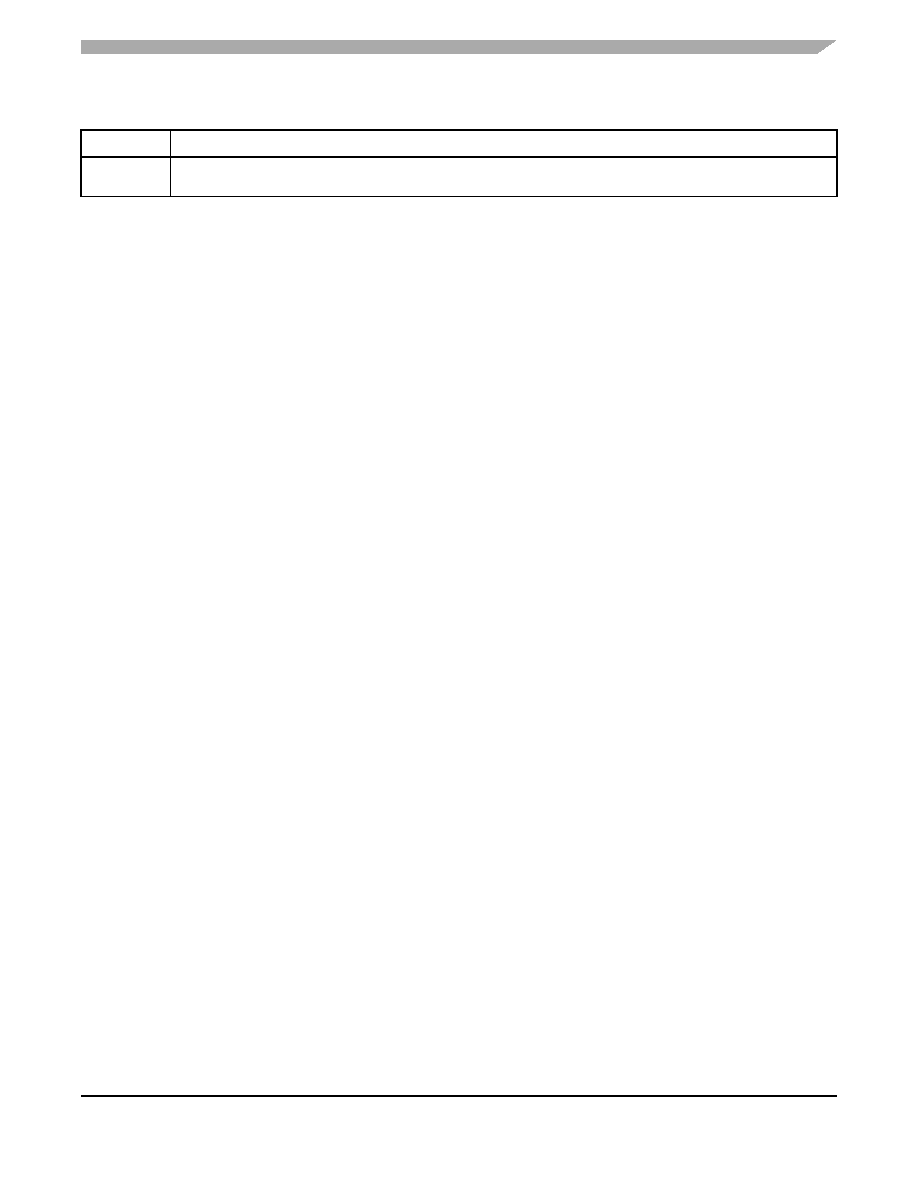
Table 254. PPAGE Field Descriptions
Field
Description
3–0
PIX[3:0]
Program Page Index Bits 3–0 — These page index bits are used to select which of the 256 P-Flash or ROM array pages is to
be accessed in the Program Page Window.
相關(guān)PDF資料 |
PDF描述 |
|---|---|
| MMC2001HCAB33B | IC MCU 32BIT 33MHZ 144-LQFP |
| MMC2107CFCPU33 | IC MCU 32BIT 33MHZ 100-LQFP |
| MMC2114CFCAG33 | IC MCU 32BIT 33MHZ 144-LQFP |
| MPC184VFB | IC SECURITY PROCESSOR 252-PBGA |
| MPC5125YVN400 | IC MCU 32BIT E300 324TEPBGA |
相關(guān)代理商/技術(shù)參數(shù) |
參數(shù)描述 |
|---|---|
| MM912H634CV1AE | 功能描述:LIN 收發(fā)器 64KS12 LIN2xLS/HS Isense RoHS:否 制造商:NXP Semiconductors 工作電源電壓: 電源電流: 最大工作溫度: 封裝 / 箱體:SO-8 |
| MM912H634CV1AER2 | 功能描述:LIN 收發(fā)器 64KS12 LIN2xLS/HS Isense RoHS:否 制造商:NXP Semiconductors 工作電源電壓: 電源電流: 最大工作溫度: 封裝 / 箱體:SO-8 |
| MM912H634DM1AE | 功能描述:16位微控制器 - MCU 64KS12 LIN2XLS/HS ISENSE RoHS:否 制造商:Texas Instruments 核心:RISC 處理器系列:MSP430FR572x 數(shù)據(jù)總線寬度:16 bit 最大時(shí)鐘頻率:24 MHz 程序存儲(chǔ)器大小:8 KB 數(shù)據(jù) RAM 大小:1 KB 片上 ADC:Yes 工作電源電壓:2 V to 3.6 V 工作溫度范圍:- 40 C to + 85 C 封裝 / 箱體:VQFN-40 安裝風(fēng)格:SMD/SMT |
| MM912H634DM1AER2 | 功能描述:16位微控制器 - MCU 64KS12 LIN2XLS/HS ISENSE RoHS:否 制造商:Texas Instruments 核心:RISC 處理器系列:MSP430FR572x 數(shù)據(jù)總線寬度:16 bit 最大時(shí)鐘頻率:24 MHz 程序存儲(chǔ)器大小:8 KB 數(shù)據(jù) RAM 大小:1 KB 片上 ADC:Yes 工作電源電壓:2 V to 3.6 V 工作溫度范圍:- 40 C to + 85 C 封裝 / 箱體:VQFN-40 安裝風(fēng)格:SMD/SMT |
| MM912H634DV1AE | 功能描述:16位微控制器 - MCU 64KS12 LIN2XLS/HS ISENSE RoHS:否 制造商:Texas Instruments 核心:RISC 處理器系列:MSP430FR572x 數(shù)據(jù)總線寬度:16 bit 最大時(shí)鐘頻率:24 MHz 程序存儲(chǔ)器大小:8 KB 數(shù)據(jù) RAM 大小:1 KB 片上 ADC:Yes 工作電源電壓:2 V to 3.6 V 工作溫度范圍:- 40 C to + 85 C 封裝 / 箱體:VQFN-40 安裝風(fēng)格:SMD/SMT |
發(fā)布緊急采購(gòu),3分鐘左右您將得到回復(fù)。