- 您現(xiàn)在的位置:買賣IC網(wǎng) > PDF目錄359153 > MCF5327 (飛思卡爾半導(dǎo)體(中國(guó))有限公司) Microprocessor Data Sheet PDF資料下載
參數(shù)資料
| 型號(hào): | MCF5327 |
| 廠商: | 飛思卡爾半導(dǎo)體(中國(guó))有限公司 |
| 英文描述: | Microprocessor Data Sheet |
| 中文描述: | 微處理器數(shù)據(jù)表 |
| 文件頁數(shù): | 28/48頁 |
| 文件大?。?/td> | 922K |
| 代理商: | MCF5327 |
第1頁第2頁第3頁第4頁第5頁第6頁第7頁第8頁第9頁第10頁第11頁第12頁第13頁第14頁第15頁第16頁第17頁第18頁第19頁第20頁第21頁第22頁第23頁第24頁第25頁第26頁第27頁當(dāng)前第28頁第29頁第30頁第31頁第32頁第33頁第34頁第35頁第36頁第37頁第38頁第39頁第40頁第41頁第42頁第43頁第44頁第45頁第46頁第47頁第48頁
MCF5329 ColdFire
Microprocessor Data Sheet, Rev. 0.1
Preliminary
Preliminary Electrical Characteristics
Freescale Semiconductor
28
5.8.2
DDR SDRAM AC Timing Characteristics
When using the SDRAM controller in DDR mode, the following timing numbers must be followed to
properly latch or drive data onto the memory bus. All timing numbers are relative to the four DQS byte
lanes. The following timing numbers are subject to change at anytime, and are only provided to aid in early
board design. Please contact your local Freescale representative if questions develop.
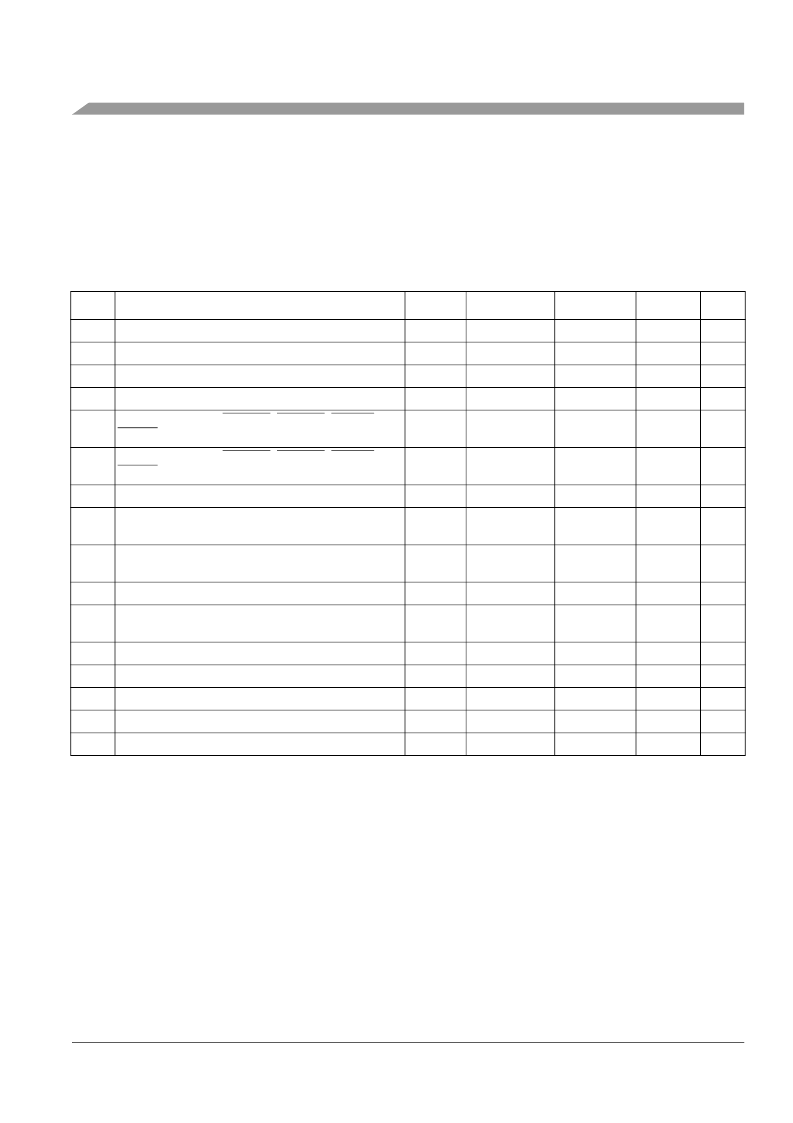
Table 12. DDR Timing Specifications
Num
Characteristic
Symbol
Min
Max
Unit
Notes
Frequency of Operation
t
DDCK
80
TBD
Mhz
1
NOTES:
1
The frequency of operation is either 2x or 4x the FB_CLK frequency of operation. FlexBus and SDRAM clock operate at the
same frequency as the internal bus clock.
2
SD_CLK is one SDRAM clock in (ns).
3
Pulse width high plus pulse width low cannot exceed min and max clock period.
4
Command output valid should be 1/2 the memory bus clock (SD_CLK) plus some minor adjustments for process,
temperature, and voltage variations.
5
This specification relates to the required input setup time of today’s DDR memories. Rigoletto’s output setup should be larger
than the input setup of the DDR memories. If it is not larger, then the input setup on the memory will be in violation.
MEM_DATA[31:24] is relative to MEM_DQS[3], MEM_DATA[23:16] is relative to MEM_DQS[2], MEM_DATA[15:8] is relative to
MEM_DQS[1], and MEM_[7:0] is relative MEM_DQS[0].
6
The first data beat will be valid before the first rising edge of DQS and after the DQS write preamble. The remaining data
beats will be valid for each subsequent DQS edge.
7
This specification relates to the required hold time of today’s DDR memories. MEM_DATA[31:24] is relative to MEM_DQS[3],
MEM_DATA[23:16] is relative to MEM_DQS[2], MEM_DATA[15:8] is relative to MEM_DQS[1], and MEM_[7:0] is relative
MEM_DQS[0].
DD1
Clock Period
t
DDSK
TBD
12.5
ns
2
DD2
Pulse Width High
t
DDCKH
0.45
0.55
SD_CLK
3
DD3
Pulse Width Low
t
DDCKL
0.45
0.55
SD_CLK
3
DD4
Address, SD_CKE, SD_CAS, SD_RAS, SD_WE,
SD_CS[1:0] - Output Valid
t
SDCHACV
—
0.5
×
SD_CLK
+ 1.0
ns
4
DD5
Address, SD_CKE, SD_CAS, SD_RAS, SD_WE,
SD_CS[1:0] - Output Hold
t
SDCHACI
2.0
—
ns
DD6
Write Command to first DQS Latching Transition
t
CMDVDQ
—
1.25
SD_CLK
DD7
Data and Data Mask Output Setup (DQ-->DQS)
Relative to DQS (DDR Write Mode)
t
DQDMV
1.5
—
ns
5
6
DD8
Data and Data Mask Output Hold (DQS-->DQ)
Relative to DQS (DDR Write Mode)
t
DQDMI
1.0
—
ns
7
DD9
Input Data Skew Relative to DQS (Input Setup)
t
DVDQ
—
1
ns
8
DD10 Input Data Hold Relative to DQS.
t
DIDQ
0.25
×
SD_CLK
+ 0.5ns
—
ns
9
DD11 DQS falling edge from SDCLK rising (output hold time) t
DQLSDCH
0.5
—
ns
DD12 DQS input read preamble width
t
DQRPRE
0.9
1.1
SD_CLK
DD13 DQS input read postamble width
t
DQRPST
0.4
0.6
SD_CLK
DD14 DQS output write preamble width
t
DQWPRE
0.25
SD_CLK
DD15 DQS output write postamble width
t
DQWPST
0.4
0.6
SD_CLK
相關(guān)PDF資料 |
PDF描述 |
|---|---|
| MCF5372 | Microprocessor Data Sheet |
| MCF5470 | MCF547x Integrated Microprocessor Electrical Characteristics |
| MCF5480 | MCF548x ColdFire㈢ Microprocessor |
| MCIMX27 | Multimedia Applications Processor(多媒體應(yīng)用處理器) |
| MCIMX31_07 | Multimedia Applications Processors |
相關(guān)代理商/技術(shù)參數(shù) |
參數(shù)描述 |
|---|---|
| MCF5327CVM240 | 功能描述:微處理器 - MPU MCF5329 V2-CORE RoHS:否 制造商:Atmel 處理器系列:SAMA5D31 核心:ARM Cortex A5 數(shù)據(jù)總線寬度:32 bit 最大時(shí)鐘頻率:536 MHz 程序存儲(chǔ)器大小:32 KB 數(shù)據(jù) RAM 大小:128 KB 接口類型:CAN, Ethernet, LIN, SPI,TWI, UART, USB 工作電源電壓:1.8 V to 3.3 V 最大工作溫度:+ 85 C 安裝風(fēng)格:SMD/SMT 封裝 / 箱體:FBGA-324 |
| MCF5327CVM240J | 制造商:Freescale Semiconductor 功能描述:MPC5XXX RISC 32-BIT CMOS 240MHZ 196-PIN MA-BGA TRAY - Trays |
| MCF5328 | 制造商:FREESCALE 制造商全稱:Freescale Semiconductor, Inc 功能描述:ColdFire㈢ Microprocessor |
| MCF53281 | 制造商:FREESCALE 制造商全稱:Freescale Semiconductor, Inc 功能描述:ColdFire㈢ Microprocessor |
| MCF53281CVM240 | 功能描述:微處理器 - MPU MCF5329 DRAGONFIRE RoHS:否 制造商:Atmel 處理器系列:SAMA5D31 核心:ARM Cortex A5 數(shù)據(jù)總線寬度:32 bit 最大時(shí)鐘頻率:536 MHz 程序存儲(chǔ)器大小:32 KB 數(shù)據(jù) RAM 大小:128 KB 接口類型:CAN, Ethernet, LIN, SPI,TWI, UART, USB 工作電源電壓:1.8 V to 3.3 V 最大工作溫度:+ 85 C 安裝風(fēng)格:SMD/SMT 封裝 / 箱體:FBGA-324 |
發(fā)布緊急采購(gòu),3分鐘左右您將得到回復(fù)。