- 您現(xiàn)在的位置:買賣IC網(wǎng) > PDF目錄45211 > MC68322FT16 (FREESCALE SEMICONDUCTOR INC) 16-BIT, 16.667 MHz, RISC PROCESSOR, PQFP160 PDF資料下載
參數(shù)資料
| 型號: | MC68322FT16 |
| 廠商: | FREESCALE SEMICONDUCTOR INC |
| 元件分類: | 微控制器/微處理器 |
| 英文描述: | 16-BIT, 16.667 MHz, RISC PROCESSOR, PQFP160 |
| 封裝: | PLASTIC, QFP-160 |
| 文件頁數(shù): | 146/283頁 |
| 文件大小: | 1602K |
| 代理商: | MC68322FT16 |
第1頁第2頁第3頁第4頁第5頁第6頁第7頁第8頁第9頁第10頁第11頁第12頁第13頁第14頁第15頁第16頁第17頁第18頁第19頁第20頁第21頁第22頁第23頁第24頁第25頁第26頁第27頁第28頁第29頁第30頁第31頁第32頁第33頁第34頁第35頁第36頁第37頁第38頁第39頁第40頁第41頁第42頁第43頁第44頁第45頁第46頁第47頁第48頁第49頁第50頁第51頁第52頁第53頁第54頁第55頁第56頁第57頁第58頁第59頁第60頁第61頁第62頁第63頁第64頁第65頁第66頁第67頁第68頁第69頁第70頁第71頁第72頁第73頁第74頁第75頁第76頁第77頁第78頁第79頁第80頁第81頁第82頁第83頁第84頁第85頁第86頁第87頁第88頁第89頁第90頁第91頁第92頁第93頁第94頁第95頁第96頁第97頁第98頁第99頁第100頁第101頁第102頁第103頁第104頁第105頁第106頁第107頁第108頁第109頁第110頁第111頁第112頁第113頁第114頁第115頁第116頁第117頁第118頁第119頁第120頁第121頁第122頁第123頁第124頁第125頁第126頁第127頁第128頁第129頁第130頁第131頁第132頁第133頁第134頁第135頁第136頁第137頁第138頁第139頁第140頁第141頁第142頁第143頁第144頁第145頁當(dāng)前第146頁第147頁第148頁第149頁第150頁第151頁第152頁第153頁第154頁第155頁第156頁第157頁第158頁第159頁第160頁第161頁第162頁第163頁第164頁第165頁第166頁第167頁第168頁第169頁第170頁第171頁第172頁第173頁第174頁第175頁第176頁第177頁第178頁第179頁第180頁第181頁第182頁第183頁第184頁第185頁第186頁第187頁第188頁第189頁第190頁第191頁第192頁第193頁第194頁第195頁第196頁第197頁第198頁第199頁第200頁第201頁第202頁第203頁第204頁第205頁第206頁第207頁第208頁第209頁第210頁第211頁第212頁第213頁第214頁第215頁第216頁第217頁第218頁第219頁第220頁第221頁第222頁第223頁第224頁第225頁第226頁第227頁第228頁第229頁第230頁第231頁第232頁第233頁第234頁第235頁第236頁第237頁第238頁第239頁第240頁第241頁第242頁第243頁第244頁第245頁第246頁第247頁第248頁第249頁第250頁第251頁第252頁第253頁第254頁第255頁第256頁第257頁第258頁第259頁第260頁第261頁第262頁第263頁第264頁第265頁第266頁第267頁第268頁第269頁第270頁第271頁第272頁第273頁第274頁第275頁第276頁第277頁第278頁第279頁第280頁第281頁第282頁第283頁
Introduction
MOTOROLA
MC68322 USER’S MANUAL
1-5
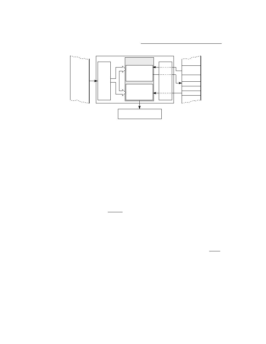
Figure 1-2. Graphics Unit Data Flow Diagram
1.2.3 Bus Interface Unit
The dual bus architecture of the MC68322 allows the printing workload to be distributed
among processing units and executed in parallel. The bus interface unit (BIU) allows the
core and graphics unit, which reside on the MC68322 bus and graphics bus, to function
independently. This is done through an arbitration unit which accommodates core accesses
to DRAM residing on the graphics bus. However, to print pages correctly, the graphics unit
gets higher priority than the core for DRAM accesses. The core performs instruction and
PROM data fetches without any impact to graphics bus operations. The BIU contains a
single-word, writeback buffer that reduces peak bus traffic generated by multiple active
modules. The writeback buffer provides a no-wait state write profile to the core and delays
the write until the graphics unit stops using the graphics bus.
1.2.4 System Integration Module
The system integration module (SIM) provides the ROM, PROM, and peripheral
chip-selects. It contains eight chip-select banks that can be programmed to decode
addresses and supply internal DTACK termination. These eight chip-select banks are
individually programmable for an address range of 256K to 64M. They can be located
anywhere within the 256M memory map and can be either contiguous or disjointed, as
required by the operating environment. Also, each chip-select bank can be independently
size or disabled.
The chip-selects for each bank can be set up to provide a wide range of timing parameters,
such as setup, access, hold, and recovery times for both read and write bus cycles. The
MC68322’s SIM provides internal bus cycle auto-acknowledge and the asynchronous WAIT
signal allows external devices to insert additional wait states as needed. The SIM also
allows SRAM to be added to the MC68322 bus for system stack space, temporary data
storage, or as a buffer for peripheral data.
MC68322
EC000
CORE
GRAPHICS UNIT
PRINT ENGINE
DRAM
DISPLAY
LIST
BAND1
BAND0
PROM
DRAM
CONTROL
RISC GRAPHICS
PROCESSOR (RGP)
PRINT ENGINE VIDEO
CONTROLLER (PVC)
F
re
e
sc
a
le
S
e
m
ic
o
n
d
u
c
to
r,
I
Freescale Semiconductor, Inc.
For More Information On This Product,
Go to: www.freescale.com
n
c
..
.
發(fā)布緊急采購,3分鐘左右您將得到回復(fù)。