- 您現(xiàn)在的位置:買賣IC網(wǎng) > PDF目錄369900 > MC33410FTA (MOTOROLA INC) DUAL CVSD/PLL CORDLESS PHONE SYSTEM PDF資料下載
參數(shù)資料
| 型號: | MC33410FTA |
| 廠商: | MOTOROLA INC |
| 元件分類: | 無繩電話/電話 |
| 英文描述: | DUAL CVSD/PLL CORDLESS PHONE SYSTEM |
| 中文描述: | TELECOM, CORDLESS, SUPPORT CIRCUIT, PQFP48 |
| 封裝: | PLASTIC, LQFP-48 |
| 文件頁數(shù): | 5/20頁 |
| 文件大小: | 300K |
| 代理商: | MC33410FTA |
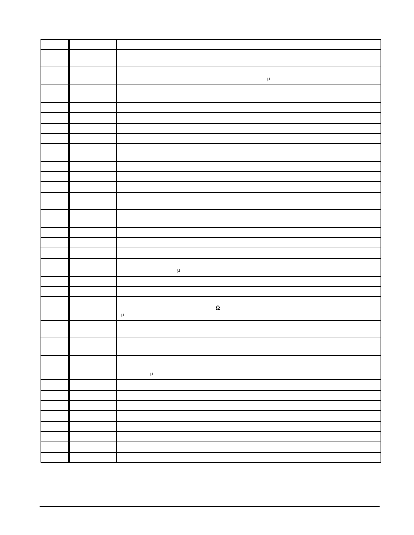
MC33410
5
MOTOROLA RF/IF DEVICE DATA
áááááááááááááááááááááááááááááááááá
16
Low Battery/CD
An open collector output. When low, indicates either the supply voltage (VCC) is low, or the carrier level is
above the threshold. This output is off when disabled.
ááááááááá
áááááááááááááááááááááááááááááááááá
17
Enc Out
The digital output of the scrambler, which passes data from the CVSD encoder, or the Tx Data register, or
the Tx 1010 Generator. Source selection is done through the P port.
18
VCC
Supply input for the audio sections, filters, and CVSD blocks. Allowable range is 2.7 to 5.5 V. Internally
connected to Pins 27 and 37.
19
Enc In
The analog input to the CVSD encoder. Max. input level is 3.0 Vpp.
Output of the transmit speech processing section.
20
Tx Audio Out
Ground
21
Ground for the audio sections, filters, and CVSD blocks. Internally connected to Pins 30 and 40.
22
MCO
Output of the microphone amplifier, and input to the filters. This output has rail–to–rail capability.
23
MCI
Inverting input of the microphone amplifier. Gain and frequency response is set with external resistors and
capacitors.
24
Enc Cap
This capacitor sets the time constant for the CVSD encoder. This pin is sensitive to leakage.
25
VAG
Analog ground for the audio section and the CVSD encoder and decoder.
26
Dec Cap
The capacitor sets the time constant for the CVSD decoder. This pin is sensitive to leakage.
27
VCC
Supply input for the audio sections, filters, and CVSD blocks. Allowable range is 2.7 to 5.5 V. Internally
connected to Pins 18 and 37.
28, 29
PAO+, PAO–
Differential outputs of the power amplifier stage for driving an earpiece or hybrid network. The gain and
frequency response are set with external resistors and capacitors.
30
Gnd
Ground for the audio sections, filters, and CVSD blocks. Internally connected to Pins 21 and 40.
31
PAI
Input to the power amplifier stage. This pin is a summing node.
32
Rx Audio Output
VB
Output of the receive speech processing section.
33
The capacitor filters the internal 1.5 V reference voltage. If VB is adjusted, it may be monitored at this pin.
Max. load current is 10 A.
34
Rx Audio In
Dec Out
Input to the receive speech processing section.
35
The analog output of the CVSD decoder.
36
MP1
As an output, provides the recovered Rx data, or the Data Detect output, or the data slicer output. Or it can
be set to a high impedance input (600 k ) for the carrier detect input signal. Selection is done through the
P port. See Table 6.
37
VCC
Supply input for the audio sections, filters, and CVSD blocks. Allowable range is 2.7 to 5.5 V. Internally
connected to Pins 18 and 27.
38
Rx Digital Input
The digital stream from the RF receiver is applied to the data slicer at this pin. Minimum amplitude is 200
mVpp. Hysteresis
≈
50 mV.
39
MP2
As an output, this pin provides the recovered clock from the Clock Recovery block. As an input, the CVSD
decoder clock can be applied to this pin. Or this pin may be set to a disabled state. Selection is done
through the P port. See Table 7. In Data Modem mode, the data to be transmitted is input to this pin.
40
Gnd
Ground for the audio sections, filters, and CVSD blocks. Internally connected to Pins 21 and 30.
41
LO2 Out
Buffered output of the 2nd LO frequency. A pullup resistor is required.
42
LO2 VCC
LO2+, LO2–
Supply pin for the 2nd LO. Allowable range is 2.7 to 5.5 V.
43, 45
A tank circuit is connected to these pins for the 2nd LO.
44
LO2 Ctl
The varactor control pin for the 2nd LO.
46
LO2 Gnd
Ground for the 2nd LO section.
47
LO2 PD
Phase detector charge pump output of the 2nd LO PLL.
48
LO2 Gnd
Ground for the 2nd LO section.
NOTE:
1. All VCC pins must be within
±
0.5 V of each other.
相關(guān)PDF資料 |
PDF描述 |
|---|---|
| MC33464N-27CTR | 30-mA Switched-Cap DC-DC Converter with fixed 2.7-V Output 6-SOT-23 -40 to 85 |
| MC33464H-09AT1 | MICROPOWER UNDERVOLTAGE SENSING CIRCUITS |
| MC33464H-09CT1 | MICROPOWER UNDERVOLTAGE SENSING CIRCUITS |
| MC33464N-09ATR | MICROPOWER UNDERVOLTAGE SENSING CIRCUITS |
| MC33464N-09CTR | MICROPOWER UNDERVOLTAGE SENSING CIRCUITS |
相關(guān)代理商/技術(shù)參數(shù) |
參數(shù)描述 |
|---|---|
| MC33412-041-11 | 制造商:SPC Multicomp 功能描述:ROCKER SWITCH SPDT CTR OFF 制造商:SPC Multicomp 功能描述:ROCKER SWITCH, SPDT, CTR OFF 制造商:SPC Multicomp 功能描述:SWITCH, ROCKER, SPDT, 15A, 250V, BLACK; Contact Configuration:SPDT; Switch Operation:On-Off-On; Contact Current Max:10A; Contact Voltage AC Nom:250V; Contact Voltage DC Nom:28V; Switch Mounting:Panel; Actuator / Cap Color:Black ;RoHS Compliant: Yes |
| MC33412-041-11 | 制造商:SPC Multicomp 功能描述:SWITCH ROCKER SPDT CTR OFF |
| MC33421 | 制造商:PRIVATE LABEL 功能描述:Axial DC Fan, 120x120x25mm, 24VDC, Ball, lead wire,Tach |
| MC33428-001-11 | 制造商:SPC Multicomp 功能描述:ROCKER SWITCH SPST BLACK 制造商:SPC Multicomp 功能描述:ROCKER SWITCH, SPST, BLACK 制造商:SPC Multicomp 功能描述:SWITCH, ROCKER, SPST, 15A, 250V, BLACK; Contact Configuration:SPST; Switch Operation:-; Contact Current Max:10A; Contact Voltage AC Nom:250V; Contact Voltage DC Nom:28V; Switch Mounting:Panel; Actuator / Cap Color:Black; Series:40 ;RoHS Compliant: Yes |
| MC33428-001-11 | 制造商:SPC Multicomp 功能描述:SWITCH ROCKER SPST BLACK |
發(fā)布緊急采購,3分鐘左右您將得到回復(fù)。