- 您現(xiàn)在的位置:買賣IC網 > PDF目錄384654 > MAX1889ETE (MAXIM INTEGRATED PRODUCTS INC) Triple-Output TFT LCD Power Supply with Fault Protection PDF資料下載
參數(shù)資料
| 型號: | MAX1889ETE |
| 廠商: | MAXIM INTEGRATED PRODUCTS INC |
| 元件分類: | 穩(wěn)壓器 |
| 英文描述: | Triple-Output TFT LCD Power Supply with Fault Protection |
| 中文描述: | 2.8 A SWITCHING REGULATOR, 1250 kHz SWITCHING FREQ-MAX, QCC16 |
| 封裝: | 5 X 5 MM, 0.80 MM HEIGHT, ULTRA THIN, QFN-16 |
| 文件頁數(shù): | 25/32頁 |
| 文件大?。?/td> | 796K |
| 代理商: | MAX1889ETE |
第1頁第2頁第3頁第4頁第5頁第6頁第7頁第8頁第9頁第10頁第11頁第12頁第13頁第14頁第15頁第16頁第17頁第18頁第19頁第20頁第21頁第22頁第23頁第24頁當前第25頁第26頁第27頁第28頁第29頁第30頁第31頁第32頁
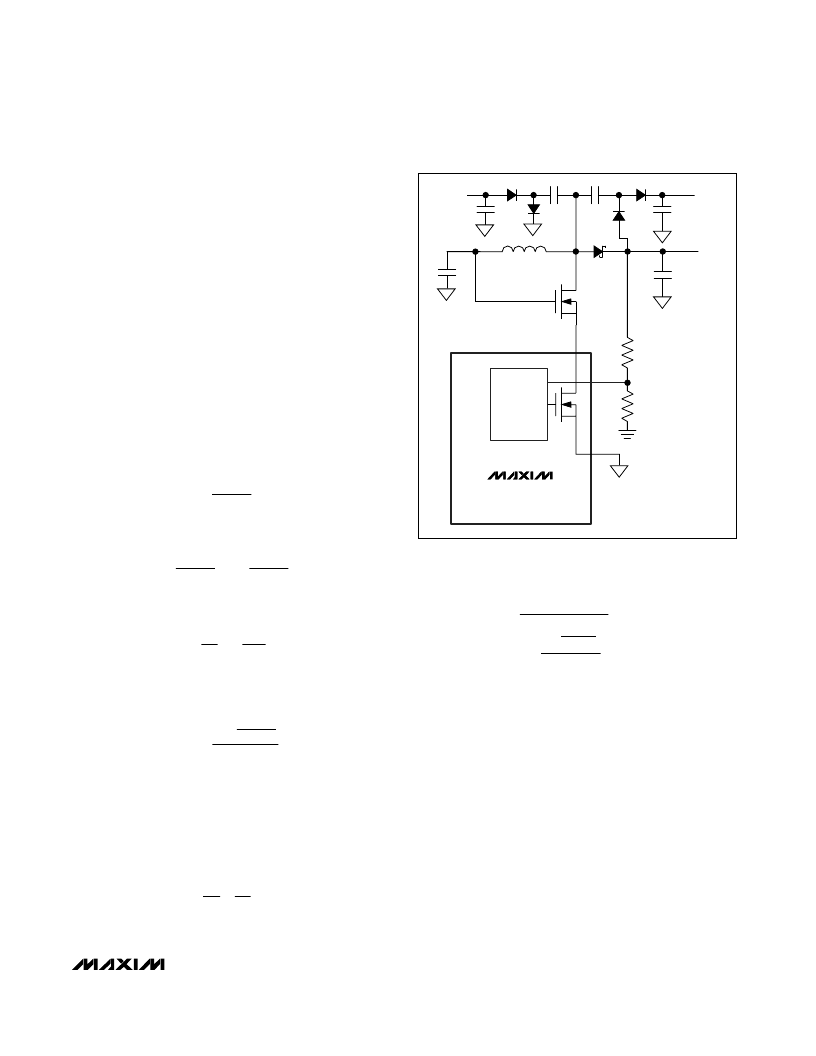
Additional Application Circuits
Operation with Output Voltage >13V
The maximum output voltage of the step-up regulator is
13V, which is limited by the absolute maximum rating of
the internal power MOSFET. To achieve higher output
voltage, an external N-channel MOSFET can be cas-
coded with the internal FET (Figure 9). Since the gate of
the external FET is biased from the input supply, use a
logic-level FET to ensure that the FET is fully enhanced
at the minimum input voltage. The current rating of the
FET needs to be higher than the internal current limit.
Changing Power-Up Sequence
The power-up sequencing of the linear regulators can be
controlled using external delays. Figure 10 shows an
application where the negative linear-regulator output
powers up with a certain delay after the positive linear
regulator reaches regulation. The resistors R1, R2, and
the capacitor C form an RC network that provides the
power-up delay. The time constant of this RC network is:
Select the ratio of R1 and R2 so that:
or:
With this R1/R2 ratio, the power-up delay can be calcu-
lated as:
where V
D
is the forward voltage drop of the diode and
0.125V is the FBN regulation point.
As a design example, assume the positive linear-regu-
lator output V
PL
is +20V, the negative charge-pump
output V
N
is -9V, and the required power-up delay time
t
D
is 4ms:
The ratio of R1 and R2 R
R
2
The required RC time constant is:
Choose C = 0.1μF, then R1//R2 = 16.8k
. Use stan-
dard resistor values: R1 = 56k
and R2 = 24k
.
Disabling Input MOSFET Switch
If the input protection MOSFET is not needed, disable
the input overcurrent comparator by connecting the
OCP pin to ground, the OCN pin to V
IN
. Leave the
GATE pin floating (Figure 11).
Generating Gamma Reference Voltage
The reference voltage for the Gamma correction resis-
tor string can be produced using the linear-regulator
controller. If the voltage difference between the main
boost voltage (V
MAIN
) and the Gamma reference volt-
age is 400mV or greater, the emitter of the PNP pass
transistor should be connected to V
MAIN
.
τ =
+
=
4
20
9
20
-
9
0 7 0 125
.
1 68
.
ms
ms
ln
.
1
9
20
=
τ
τ
D
PL
V
V
D
R
+
R
0 125
R
V
=
ln
.
1
1
2
-
R
R
V
V
N
PL
1
2
=
-
V
R
+
R
R
V
R
+
R
R
N
PL
2
1
2
1
1
2
0
+
=
τ =
×
+
R
R
R
R
C
1
1
2
2
M
Triple-Output TFT LCD Power Supply
with Fault Protection
______________________________________________________________________________________
25
STEP-UP
REGULATOR
LX
FB
PGND
MAX1889
V
N
V
P
V
MAIN
15V
V
IN
Figure 9. Operation with Output Voltage >13V Using Cascoded
MOSFET
相關PDF資料 |
PDF描述 |
|---|---|
| MAX1889 | Fixed-Point Digital Signal Processor 256-BGA |
| MAX1896 | 1.4MHz SOT23 Current-Mode Step-Up DC-DC Converter |
| MAX1896EUT-T | Fixed-Point Digital Signal Processor 532-FCBGA |
| MAX1898 | Fixed-Point Digital Signal Processor 532-FCBGA |
| MAX1898EUB41 | Linear Charger for Single-Cell Li Battery |
相關代理商/技術參數(shù) |
參數(shù)描述 |
|---|---|
| MAX1889ETE+ | 功能描述:直流/直流開關轉換器 Quad-Output TFT LCD Power Supply RoHS:否 制造商:STMicroelectronics 最大輸入電壓:4.5 V 開關頻率:1.5 MHz 輸出電壓:4.6 V 輸出電流:250 mA 輸出端數(shù)量:2 最大工作溫度:+ 85 C 安裝風格:SMD/SMT |
| MAX1889ETE+T | 功能描述:LCD 驅動器 Quad-Output TFT LCD Power Supply RoHS:否 制造商:Maxim Integrated 數(shù)位數(shù)量:4.5 片段數(shù)量:30 最大時鐘頻率:19 KHz 工作電源電壓:3 V to 3.6 V 最大工作溫度:+ 85 C 最小工作溫度:- 20 C 封裝 / 箱體:PDIP-40 封裝:Tube |
| MAX1889ETE-T | 功能描述:LCD 驅動器 RoHS:否 制造商:Maxim Integrated 數(shù)位數(shù)量:4.5 片段數(shù)量:30 最大時鐘頻率:19 KHz 工作電源電壓:3 V to 3.6 V 最大工作溫度:+ 85 C 最小工作溫度:- 20 C 封裝 / 箱體:PDIP-40 封裝:Tube |
| MAX1889EVKIT | 功能描述:電源管理IC開發(fā)工具 MAX1889 Eval Kit RoHS:否 制造商:Maxim Integrated 產品:Evaluation Kits 類型:Battery Management 工具用于評估:MAX17710GB 輸入電壓: 輸出電壓:1.8 V |
| MAX188ACAP | 功能描述:模數(shù)轉換器 - ADC Integrated Circuits (ICs) RoHS:否 制造商:Texas Instruments 通道數(shù)量:2 結構:Sigma-Delta 轉換速率:125 SPs to 8 KSPs 分辨率:24 bit 輸入類型:Differential 信噪比:107 dB 接口類型:SPI 工作電源電壓:1.7 V to 3.6 V, 2.7 V to 5.25 V 最大工作溫度:+ 85 C 安裝風格:SMD/SMT 封裝 / 箱體:VQFN-32 |
發(fā)布緊急采購,3分鐘左右您將得到回復。